Het PCB lamineerproces is een kritieke stap in de productie van printplaten met meerdere lagen. Hierbij worden geleidende lagen (koperfolie), isolerende lagen (prepreg) en substraatmaterialen onder hoge temperatuur en druk permanent aan elkaar gehecht om een meerlagige circuitstructuur te vormen met interconnecties met een hoge dichtheid. Dit proces bepaalt rechtstreeks de mechanische sterkte, elektrische prestaties en betrouwbaarheid op lange termijn van PCB's en dient als de technische basis voor de miniaturisatie en hoogfrequente ontwikkeling van moderne elektronische apparaten.
Basisprincipes en functies van het PCB lamineerproces
Het lamineerproces maakt in wezen gebruik van de vloei- en uithardingseigenschappen van thermohardende harsen onder hoge temperatuur om een permanente hechting van meerlaagse materialen te bereiken in een nauwkeurig gecontroleerde drukomgeving. De belangrijkste functies zijn:
- Elektrische aansluiting: Maakt verticale verbindingen mogelijk tussen circuits op verschillende lagen, waardoor de fysieke basis wordt gelegd voor complexe bedrading.
- Mechanische ondersteuningBiedt structurele stijfheid en dimensionale stabiliteit voor printplaten.
- Isolatiebescherming: Isoleert verschillende geleidende lagen door middel van diëlektrische materialen om kortsluiting te voorkomen.
- Thermisch beheerOptimaliseert de warmteafvoer door materiaalkeuze en laminaatstructuur.
Systeem voor lamineermateriaal
Samenstelling kernmateriaal
| Type materiaal | Belangrijkste functie | Algemene specificaties | Speciale varianten |
|---|
| Substraat Kern | Biedt mechanische ondersteuning en basisisolatie | FR-4, dikte 0,1-1,6 mm | Hoge-Tg FR-4, hoogfrequent materialen (Rogers-serie) |
| Prepreg (PP) | Tussenlaagverlijming en isolatie | 106/1080/2116, enz., harsinhoud 50-65% | Lage stroom, hoge hittebestendigheid |
| Koperfolie | Geleidende laagvorming | 1/2 oz-3 oz (18-105 μm) | Omgekeerd behandelde folie, folie met laag profiel |
Overwegingen bij materiaalselectie
- Glasovergangstemperatuur (Tg): Standaard FR-4 is 130-140 °C, terwijl materialen met een hoge Tg 170-180 °C kunnen bereiken.
- Diëlektrische constante (Dk): Snelle circuits vereisen materialen met een laag Dk-gehalte (3,0-3,5).
- Dissipatiefactor (Df): Hoogfrequente toepassingen vereisen Df < 0,005.
- Thermische uitzettingscoëfficiënt (CTE): De CTE van de Z-as moet lager zijn dan 50 ppm/°C om scheuren in de via's te voorkomen.
Gedetailleerde lamineerprocesstroom
1. Voorbehandelingsfase
- MateriaalvoorbereidingMateriaalmodellen en batchnummers controleren, harsinhoud en stroom meten.
- Behandeling van de binnenlaag: Oxideren om de oppervlakteruwheid te verhogen en de hechting te verbeteren.
- Stack-Up Ontwerp: Volg de symmetrieprincipes om kromtrekken als gevolg van een CTE-mismatch te voorkomen.
2.Stapelen en uitlijnen
- Uitlijnsysteem: Gebruik gaten met vier sleuven (+0,1 mm tolerantie) of röntgenuitlijningssystemen (nauwkeurigheid ±15 μm).
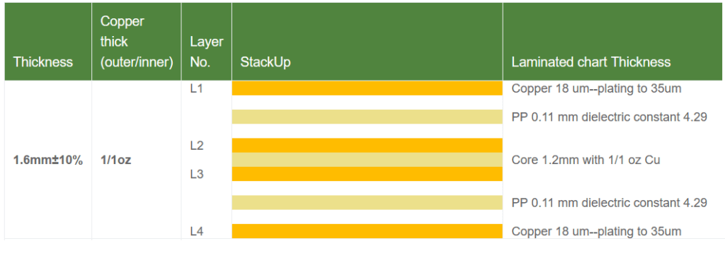
- Stapelvolgorde: Typische 8-lagen structuur: koperfolie-PP-kern-PP-kern-PP-koperfolie.
3.Parameterregeling lamineercyclus
| Parameter | Controlebereik | Impact |
|---|
| Verwarmingssnelheid | 2-3 °C/min | Te snel veroorzaakt ongelijkmatige uitharding van hars; te langzaam vermindert de efficiëntie. |
| Lamineringstemperatuur | 180-200 °C | Te hoog degradeert de hars; te laag resulteert in onvolledige uitharding. |
| Druk Toepassing | 200-350 PSI | Een te hoge waarde veroorzaakt een overmatige harsstroom; een te lage waarde vermindert de hechting. |
| Vacuümniveau | ≤50 mbar | Verwijdert vluchtige stoffen en restlucht. |
| Uithardingstijd | 60-120 min | Zorgt voor volledige crosslinking van hars. |
4.Nabehandeling en koeling
- Stap Koeling: Regel de afkoelsnelheid (1-2 °C/min) om interne spanning te verminderen.
- Verlichting van stress: Houd de temperatuur enige tijd onder Tg om de restspanning te verminderen.
 Meerlagige PCB
Analyse en tegenmaatregelen voor gemeenschappelijke lamineerproblemen
Delaminatie en holtes
- OorzakenOnvoldoende harsstroom, achtergebleven vluchtige stoffen, materiaalvervuiling.
- OplossingenOptimaliseer de verwarmingscurve, voeg een vacuümontgassing toe en regel de omgevingsvochtigheid strikt (<40% RH).
Scheeftrekken
- OorzakenCTE-afwijking, ongelijke druk, te hoge afkoelsnelheid.
- OplossingenKies voor symmetrisch ontwerp, optimaliseer de drukverdeling en regel de koelsnelheid.
Harsgebrek en blootstelling aan glasweefsel
- OorzakenOvermatige harsstroom, overmatige druk.
- OplossingenKies PP met laag debiet, optimaliseer de drukcurve, gebruik stuwbalken.
Geavanceerde lamineertechnologieën
Lamineren met vacuümondersteuning
Vacuümondersteunde lamineertechnologie verbetert de hechtingskwaliteit tussen de lagen van meerlaagse printplaten aanzienlijk door het proces in een volledige vacuümomgeving (≤5 mbar) uit te voeren. Deze techniek verwijdert effectief lucht en vluchtige stoffen tussen de lagen tijdens het persen, waardoor het percentage defecten als gevolg van luchtbellen wordt teruggebracht van de traditionele 5-8% tot minder dan 1%.Deze techniek is met name geschikt voor de productie van hoogfrequente printplaten en dikke koperen printplaten, omdat deze een extreem hoge consistentie in diëlektrische eigenschappen en thermische geleidbaarheid tussen de lagen vereisen. De vacuümomgeving zorgt ervoor dat de hars tijdens de vloeifase de openingen in het circuit volledig opvult, waardoor een uniforme diëlektrische laag wordt gevormd die het transmissieverlies van hoogfrequente signalen met 15-20% vermindert.Bij toepassingen met dik koper (≥3 oz) voorkomt vacuümondersteuning effectief delaminatie als gevolg van oneffenheden in de koperfolie, waardoor de afpelsterkte tussen de lagen toeneemt tot meer dan 1,8 N/mm. Moderne vacuümlamineerapparatuur is ook uitgerust met realtime druksensoren met 128 meetpunten, die zorgen voor een drukuniformiteit binnen ±5%, wat de consistentie van de productie aanzienlijk verbetert.
Sequentiële lamineertechnologie
Sequentiële lamineertechnologie maakt de productie van zeer complexe meerlaagse printplaten mogelijk door middel van meerdere persfasen. Bij dit proces worden eerst de binnenste kernlagen gelamineerd met gedeeltelijke prepreg om submodules te vormen, gevolgd door boren, plateren en andere processen om verbindingen tot stand te brengen. Ten slotte worden de resterende lagen toegevoegd in een tweede lamineerproces.Door deze stapsgewijze aanpak kunnen passieve componenten (zoals weerstanden en condensatoren) en speciale functionele lagen (bijvoorbeeld thermisch geleidende metalen substraten) tussen de lagen worden ingebed, waardoor systeem-in-pakket-integratie mogelijk wordt. Bij de productie van hoogwaardige PCB's met 16 of meer lagen controleert sequentiële laminering de uitlijningsnauwkeurigheid tussen de lagen binnen ±25 µm, terwijl cumulatieve spanning die bij persen in één stap ontstaat, wordt vermeden.Bovendien ondersteunt deze technologie hybride diëlektrische structuren, bijvoorbeeld door gebruik te maken van materialen met een laag verlies (zoals gemodificeerd polyimide) voor hogesnelheidssignaal-lagen en materialen met een hoge thermische geleidbaarheid voor vermogenslagen, waardoor het invoegverlies voor 56 Gbps hogesnelheidssignalen met 0,8 dB/cm wordt verminderd.Hoewel de productiecyclus met 30% toeneemt, verbetert het rendement tot 98,5%, waardoor deze technologie bijzonder geschikt is voor PCB's die worden gebruikt in 5G-communicatieapparatuur en high-end servers.
Lamineerproces bij lage temperatuur
Het lamineerproces bij lage temperatuur maakt gebruik van speciaal aangepaste harssystemen om het lamineren bij lagere temperaturen van 130-150 °C te voltooien, wat 40-50 °C lager is dan bij conventionele methoden. Door het moleculaire ontwerp van epoxyharsen en de optimalisatie van katalytische systemen bereikt de hars volledige verknoping bij lagere temperaturen, terwijl een Tg-waarde van ≥160 °C behouden blijft.Het belangrijkste voordeel is een aanzienlijke vermindering van de thermische belasting op gevoelige componenten, waardoor materiaalvervorming en prestatieverlies als gevolg van hoge temperaturen worden voorkomen.Bij de productie van flexibele printplaten en rigide-flexibele printplaten beperkt lamineren bij lage temperatuur de krimp van polyimidesubstraten tot minder dan 0,05% en vermindert het de verkeerde uitlijning van circuits tot ±15 µm. Bovendien verlaagt dit proces het energieverbruik (besparing van meer dan 30%) en de CO₂-uitstoot aanzienlijk, wat in overeenstemming is met de eisen voor groene productie.De nieuwste ontwikkelingen hebben betrekking op met nano-vulstoffen versterkte lage-temperatuurharsen (bijvoorbeeld met silica-nanodeeltjes), die de thermische uitzettingscoëfficiënt (CTE) tussen de lagen verminderen tot 35 ppm/°C, waardoor ze voldoen aan de betrouwbaarheidseisen van auto-elektronica in omgevingen van -40 °C tot 150 °C.
Kwaliteitscontrole en inspectie
Destructief testen
- Microsectie-analyse: Controleert de hechting tussen de lagen, de harsvulling en de kwaliteit van de gatenwand.
- Peel Sterkte Test: Evalueert de hechting tussen koperfolie en substraat (standaardvereiste ≥1,0 N/mm).
- Thermische stresstest: Dompel gedurende 10 seconden onder in 288 °C soldeer om te controleren op delaminatie.
Niet-destructief onderzoek
- Ultrasoon scannen: Detecteert interne holtes en delaminatiedefecten.
- RöntgeninspectieEvalueert de uitlijningsnauwkeurigheid tussen lagen en de positionering van ingesloten componenten.
- Diëlektrische Sterkte Test: Controleert de isolatieprestaties tussen de lagen.
Trends in lamineerprocessen
- MateriaalinnovatieNano-gevulde gemodificeerde harsen, hoogfrequente materialen met laag verlies, milieuvriendelijke halogeenvrije substraten.
- Verfijning van processen: Real-time druk-temperatuurbewaking, AI-parameteroptimalisatie, digitale tweelingtechnologie.
- Inlichtingen over apparatuur: Geïntegreerde sensornetwerken, adaptieve regelsystemen, diagnose op afstand en onderhoud.
- Duurzame ontwikkeling: Verminder het energieverbruik met meer dan 30%, minimaliseer VOC-emissies en verbeter het materiaalgebruik.
Toepassingsspecifieke vereisten
| Toepassingsveld | Speciale lamineervereisten | Typische lamineeroplossing |
|---|
| Automobielelektronica | Hoge betrouwbaarheid, bestand tegen thermische cycli | Hoge-Tg materialen, verbeterde harssystemen |
| 5G-communicatie | Laag verlies, stabiele Dk/Df | Hoogfrequente speciale materialen, strenge controle op harsinhoud |
| Ruimtevaart | Aanpassingsvermogen aan extreme omgevingen | Polyimidesubstraten, lamineerprocessen bij hoge temperaturen |
| Consumentenelektronica | Dun, hoge dichtheid | Ultradunne kernen, nauwkeurige harscontrole |
Conclusie
Het PCB-lamineerproces, de belangrijkste stap in de productie van printplaten met meerdere lagen, bepaalt rechtstreeks de prestaties en betrouwbaarheid van het eindproduct. Naarmate elektronische apparaten zich ontwikkelen in de richting van hogere frequenties, snelheden en dichtheden, ontwikkelt de lamineertechnologie zich in de richting van grotere precisie, intelligentie en milieuduurzaamheid. Het beheersen van de principes, materialen en parametercontrole van lamineren is cruciaal voor zowel PCB-ontwerp als hoogwaardige productie.