Description
Double-sided Flexible Printed Circuit Boards, DS-FPC for short, are circuit boards with conductive graphics laid on both sides of an insulating substrate. This type of circuit board connects the graphics on both sides through metalized holes to form a conductive path, thus meeting the design requirements of flexibility.
Structural Features
The main features of Double-Sided Flexible Printed Circuit Boards include
Double-Sided Routing: The conductive graphics are etched on both sides of the insulating substrate, and the graphics are connected to form a conductive path through metalized holes. Connect the two sides of the graphic to form a conductive path
Protective overlay film: used to protect single and double-sided conductors and indicate the placement of components
Parameters of double-sided flexible printed circuit boards
| Item |
Flexible PCB |
| Max Layer |
2L |
| Inner Layer Min Trace/Space |
3/3mil |
| Out Layer Min Trace/Space |
3.5/4mil |
| Inner Layer Max Copper |
2oz |
| Out Layer Max Copper |
2oz |
| Min Mechanical Drilling |
0.1mm |
| Min Laser Drilling |
0.1mm |
| Aspect Ratio(Mechanical Drilling) |
10:1 |
| Aspect Ratio(Laser Drilling) |
/ |
| Press Fit Hole Ttolerance |
±0.05mm |
| PTH Tolerance |
±0.075mm |
| NPTH Tolerance |
±0.05mm |
| Countersink Tolerance |
±0.15mm |
| Board Thickness |
0.1-0.5mm |
| Board Thickness Tolerance(<1.0mm) |
±0.05mm |
| Board Thickness Tolerance(≥1.0mm) |
/ |
| Impedance Tolerance |
Single-Ended:±5Ω(≤50Ω),±10%(>50Ω) |
| Differential:±5Ω(≤50Ω),±10%(>50Ω) |
| Min Board Size |
5*10mm |
| Max Board Size |
9*14inch |
| Contour Tolerance |
±0.05mm |
| Min BGA |
7mil |
| Min SMT |
7*10mil |
| Surface Treatment |
ENIG, Gold Finger, Immersion Silver, Immersion Tin, HASL(LF), OSP, ENEPIG, Flash Gold; Hard gold plating |
| Solder Mask |
Green Solder Mask/Black PI/Yellow PI |
| Min Solder Mask Clearance |
3mil |
| Min Solder Mask Dam |
8mil |
| Legend |
White, Black, Red, Yellow |
| Min Legend Width/Height |
4/23mil |
| Strain Fillet Width |
1.5+0.5mil |
| Bow & Twist |
/ |
Key Advantages of Double-Sided Flexible Printed Circuits (Double-Sided FPCs)
Building upon single-sided FPCs, double-sided flexible circuits incorporate an additional conductive layer, significantly expanding design flexibility and functional integration. Their core advantages include:
1. High-Density Interconnect Design
-
Dual-layer routing doubles wiring density, supporting more complex circuit topologies
-
Microvia technology enables precise interlayer connections (minimum aperture: 50μm)
-
Ideal for integrating high-pin-count ICs and fine-pitch components (<0.3mm)
2. Maximized Space Efficiency
-
3D stacked routing saves over 40% space compared to single-sided FPCs
-
Foldable/rollable installations enable compact layouts in three-dimensional spaces (e.g., hinge-based devices)
-
Replaces multiple rigid PCBs, reducing connector count by 60%
3. Enhanced Electrical Performance
-
Dual-sided ground layers reduce signal crosstalk and EMI radiation by 30%
-
Supports differential pair routing, improving high-speed signal integrity (for 5G/high-frequency applications)
-
Optional shielding layers (copper foil/conductive ink) meet military-grade EMC requirements
4. Upgraded Mechanical Reliability
-
Symmetrical structure design balances stress distribution, increasing bending cycles by 50% vs. single-sided FPCs
-
Double-layer lamination (PI/PET + copper foil) enhances tear resistance
-
Passes dynamic bending tests (>500,000 cycles @ R=1mm)
5. Multi-Functional Integration Potential
-
Double-sided SMT assembly: Components can be mounted on both sides for modular integration
-
Hybrid rigid-flex design: Reinforced sections (FR4 stiffeners) support heavy components
-
Embedded components: Resistors/capacitors buried between layers further reduce thickness
Key Design Considerations for Double-Sided Flexible Printed Circuits (FPCs)
1. Minimum Bend Radius Design
The minimum bend radius (Rmin) is a critical parameter in double-sided FPC design. It is calculated as:
Rmin = C × t
Where:
Design Guidelines:
| Application Type |
Empirical Coefficient (C) |
Practical Minimum Radius |
| Static bending (fixed installations) |
6–10 |
≥2× board thickness |
| Dynamic bending (repeated flexing) |
20–40 |
≥10× board thickness |
Material Impact:
2. Signal Integrity & EMI Control
-
Routing optimization:
-
Minimize signal path length
-
Avoid sharp 90° turns (>45° preferred)
-
Limit via count to reduce reflections
-
Impedance management:
-
Power distribution:
3. Mechanical Reinforcement Strategies
-
Bending zone design:
-
Route traces parallel to the bend axis
-
Eliminate vias in flex areas
-
Use radial transitions (no sharp corners)
-
Stress relief features:
-
Apply PI stiffeners at the connector interfaces
-
Add FR4 reinforcements in high-stress regions
-
Implement tapered coverlay edges
4. Advanced Material Selection
| Component |
Recommended Options |
Key Benefit |
| Conductor |
Rolled annealed copper (RA) |
Superior flex endurance |
| Dielectric |
Polyimide (up to 200°C rating) |
High temp stability |
| Adhesive |
Acrylic or epoxy-modified systems |
Balanced flexibility/adhesion |
5. Multilayer Design Considerations
-
Layer stacking:
-
Via management:
6. Thermal Management Solutions
-
High-power applications:
-
Embed thermal vias under heat-generating components
-
Integrate aluminum heat spreaders in rigid sections
-
Use thermally conductive adhesives (≥3 W/mK)
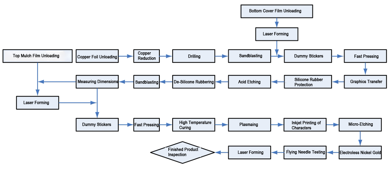
Double-Sided FPCs Manufacturing Process
The manufacturing process for double-sided flexible printed circuit boards consists of the following major steps:
Substrate Preparation: Selection of a suitable insulating substrate, such as polyimide (PI) or polyester (PET).
Wiring Etching: Wiring etching is performed on each of the two sides of the substrate to form a conductive pattern.
Metallized Hole Production: Form metalized holes on the substrate through drilling and plating processes to achieve conductive connections between different layers.
Covering Film Covering: Cover the wiring and metalized holes with a protective film to ensure the stability and durability of wires and connecting points to ensure the stability and durability of wires and connecting points
Application Scenarios
Double-sided Flex PCBs are widely used in a variety of applications where flexibility and reliability are required, including but not limited to:
Consumer Electronics: such as flexible connectors in devices such as smartphones and tablets.
Automotive electronics: In various sensors and controllers inside automobiles, double-sided flex PCBs can provide better bending and vibration tolerance.
Industrial Controls: In automation equipment and robotics, double-sided flex PCBs can accommodate complex mechanical movements and space constraints.

Why choose us?
1. One-stop PCB PCBA Service
We can help you with a one-stop service. To support you with the whole process from function research and development, product design discussion, PCB manufacturing, and component procurement to PCB assembly.
2. Advanced Equipment
There is more than 385 equipment, mainly imported from Germany, Japan, and Taiwan. Such as LDl automatic exposure machine, automatic plating line, laser drilling machine, automatic testing machine, automatic V-cutting machine, and other advanced equipment.
3 . Advanced Technology
There are more than 28 employees on our R&D team, including 2 doctoral students and 8 master’s students. We can do 3 3-step HDI PCBs and 0.4mm pitch holes. Technology is in the leading position in the industry.
4. Superior Service
7*24-hour online service! We have a professional service team to follow the whole process for key customers and keywords. Also, we have a professional account manager for each customer to meet the customer’s various demands.