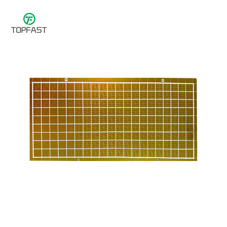
Description
Power Lighting PCBs are printed circuit boards (PCBs) used in power and lighting equipment, whose main roles are to provide electrical connections, support electronic components, and enable signal transmission and energy distribution.
Product Definition & Core Functions
Power lighting PCBs are printed circuit boards specifically designed for power electronics and lighting systems, featuring three core functions:
-
High-Precision Electrical Interconnection
-
Supports current density up to 10A/mm²
-
Enables multi-layer signal transmission (control/feedback/power loops)
-
±5% impedance control accuracy
-
Enhanced Mechanical Support
-
Complies with IPC-A-610 Class 2 standards
-
Vibration-resistant design (passed 5Grms random vibration test)
-
Supports SMT/THT hybrid assembly processes
-
Intelligent Power Management
-
Multi-layer stacked power plane design
-
Integrated PDN (Power Delivery Network) optimization
-
Supports 12V/24V/48V multi-voltage domain management
There are three main types of ceramic PCBs available, each with its unique characteristics.
HTCC (High-Temperature Co-fired Ceramic) requires the ceramic powder to be heated up to 1300-1600? With no glass material added.
LTCC (Low-Temperature Co-fired Ceramic) requires a mix of inorganic alumina powder with about 30-50% glass material and an organic binder.
DBC (Direct Bonded Copper) uses a copper oxygen-containing eutectic liquid to create a chemical reaction between the substrate and copper foil and form a CuAlO2 or CuAl2O4 phase. Different applications and requirements determine which type of ceramic PCB should be used.
How to Produce the Ceramic PCB?
Producing ceramic PCBs requires precision and care in the manufacturing process. First, metal elements or substrates are placed in each layer with a layer-by-layer screen printing process. Then, conductive paste such as silver or gold is used to place trace connections. It is also possible to punch or laser drill holes in the unburned layer. Afterwards, the entire stack is baked in an oven at a temperature of below 1000°C, which matches the firing temperature of the gold and silver paste used. Finally, laser processing is applied to drill or cut micro-holes in the ceramic layer. Such a precise and intricate procedure allows for high-quality ceramic PCBs without any defects.
Technical Advantage Comparison
| Performance Metric |
Traditional Solution |
Modern Power Lighting PCB |
| Conversion Efficiency |
85% |
≥95% |
| Power Density |
3W/cm³ |
10W/cm³ |
| Response Time |
100ms |
<1ms |
| Operating Temp Range |
0℃~70℃ |
-40℃~125℃ |
| MTBF |
50,000 hours |
100,000 hours |
Innovative Technology Highlights
-
High-Frequency Transformer Technology
-
Operating frequency up to 500kHz
-
Volume reduced to 1/8 of traditional solutions
-
15% improvement in conversion efficiency
-
Intelligent Monitoring System
-
Advanced Thermal Management
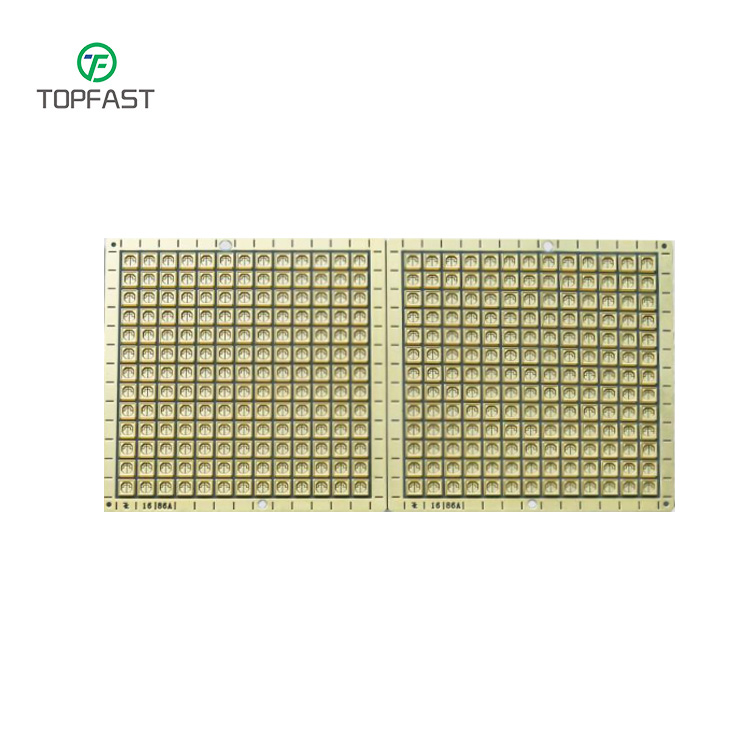
Power Supply Lighting PCB Parameters
| thickness of the ceramic |
0.38/0.50mm |
| Shipment length and width dimensions |
109.2*54.5mm |
| The aperture size |
≥0.07mm |
| Hole spacing |
≥0.25mm |
| The line width |
≥0.15mm |
| The channel width |
≥0.11mm |
| DAMS width |
0.2mm |
| Around the dam height |
0.6mm |
| Resistance welding type |
Green, White, Black |
Primary Application Areas
-
Power Electronics
-
IGBT power modules
-
High-current MOSFET arrays
-
Solid-state relay systems
-
EV power converters (SiC/GaN devices)
-
RF & Microwave Systems
-
5G base station amplifiers
-
Radar system front-ends
-
Satellite communication modules
-
RF power combiners (up to 40GHz)
-
Automotive Electronics
-
Industrial Systems
-
Aerospace & Defense
Emerging Applications:
• Quantum computing cryogenic interfaces
• Fusion reactor monitoring systems
• Direct-bonded copper power modules
• Ultra-high frequency surgical equipment
With continuous material advancements, ceramic PCBs are expanding into new frontiers of electronics where reliability under extreme conditions is paramount. Their unique combination of thermal, electrical, and mechanical properties makes them the substrate of choice for mission-critical applications across multiple industries.