الحفر هو العملية التي يحول النحاس المطلي إلى أنماط دوائر كهربائية دقيقة.
على الرغم من أن الأمر يبدو بسيطاً ظاهرياً، إلا أن الحفر هو أحد الخطوات الأكثر حساسية للإنتاجية في تصنيع ثنائي الفينيل متعدد الكلور.
من وجهة نظر الشركة المصنّعة، يؤدي ضعف التحكم في الحفر إلى:
- تباين عرض الخط
- السراويل القصيرة والمفتوحة
- عائد منخفض
- ارتفاع تكلفة التصنيع
تشرح هذه المقالة كيفية عمل النقش على ثنائي الفينيل متعدد الكلور، وما الذي يؤثر على جودة النقش، وكيف يمكن للمصنعين مثل توب فاست التحكم في الإنتاجية لضمان إنتاج مركبات ثنائي الفينيل متعدد الكلور بشكل متسق وفعال من حيث التكلفة.
جدول المحتويات
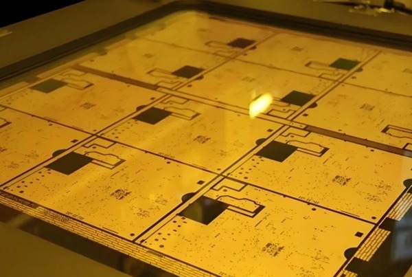
ما هو نقش ثنائي الفينيل متعدد الكلور؟
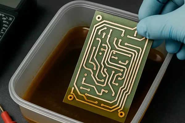
حفر ثنائي الفينيل متعدد الكلور هو عملية كيميائية يزيل النحاس غير المرغوب فيه من اللوحة، تاركًا فقط نمط الدائرة المصمم.
يتم تطبيق الحفر على:
- الطبقات الداخلية
- الطبقات الخارجية
الهدف هو تحقيق عرض التتبع الدقيق، والتباعد، والهندسة الدقيقة وفقًا لمواصفات التصميم.
أنواع عمليات نقش ثنائي الفينيل متعدد الكلور
حفر الطبقة الداخلية
يحدث نقش الطبقة الداخلية:
- قبل التصفيح
- على رقائق نحاسية رقيقة
إنها حساسة للغاية لأن:
- لا يمكن إصلاح العيوب بعد التصفيح
- يؤثر مردود الطبقة الداخلية على مكدس ثنائي الفينيل متعدد الكلور بالكامل
نقش الطبقة الخارجية
يحدث نقش الطبقة الخارجية:
- بعد طلاء النحاس
- على طبقات النحاس السميكة
يجب أن يأخذ نقش الطبقة الخارجية في الحسبان:
- سُمك النحاس المطلي
- التوحيد عبر اللوحة
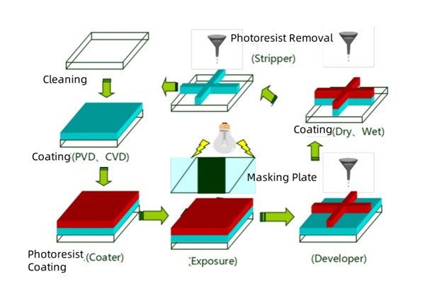
عملية حفر ثنائي الفينيل متعدد الكلور خطوة بخطوة
الخطوة 1 - إعداد نمط المقاومة
طبقة مقاومة تحمي المناطق النحاسية التي يجب أن تبقى بعد الحفر.
تحدد دقة النمط في هذه المرحلة هندسة التتبع النهائي.
الخطوة 2 - الحفر الكيميائي
تزيل المحاليل الكيميائية النحاس المكشوف بشكل انتقائي.
متغيرات العملية الرئيسية:
- تركيز المادة المثرية
- درجة الحرارة
- ضغط الرذاذ
- وقت الحفر
يعد التحكم في هذه المتغيرات أمرًا ضروريًا لتحقيق نتائج مستقرة.
الخطوة 3 - مقاومة التعرية
بعد الحفر، تتم إزالة المقاومة المتبقية لتظهر الآثار النحاسية النهائية.
عيوب الحفر الشائعة وتأثيرها
الحفر الزائد
الأسباب:
- وقت الحفر المفرط
- الكيمياء العدوانية
النتائج:
- تقليل عرض التتبع
- زيادة المعاوقة
- تفتح الاحتمالات
نقش تحت الحفر
الأسباب:
- وقت الحفر غير كافٍ
- ضعف نشاط الإيثلين
النتائج:
- النحاس المتبقي
- شورتات بين الآثار
التقويض
تزيل مادة الحفر النحاس جانبياً تحت المقاومة، مما يقلل من عرض الأثر.
يصبح التقويض أكثر حدة مع:
- نحاس سميك
- تصميمات تتبع أدق التصاميم
ما هو العائد في تصنيع ثنائي الفينيل متعدد الكلور؟
يشير العائد إلى النسبة المئوية للوحات التي تستوفي المواصفات بعد التصنيع.
العائد المرتفع يعني:
- تكلفة أقل لكل وحدة
- جودة مستقرة
- تسليم يمكن التنبؤ به
يؤدي انخفاض العائد المنخفض إلى:
- الخردة
- إعادة العمل
- تكلفة إجمالية أعلى
كيف يؤثر الحفر على إنتاجية التصنيع
يؤثر الحفر مباشرة على المحصول لأن:
- تتسبب عيوب التتبع في حدوث عطل كهربائي
- تتضاعف عيوب الطبقة الداخلية عبر اللوحات
- تؤثر الاختلافات الصغيرة على التصميمات عالية الكثافة
من وجهة نظر الشركة المصنعة، يعد الحفر أحد أعلى نقاط رفع مالي لتحسين المحصول.
عوامل التصميم التي تؤثر على إنتاجية النقش
يتحسن العائد عند التصميمات:
- تجنب الآثار الدقيقة غير الضرورية
- الحفاظ على اتساق عرض الخط
- توزيع النحاس المتوازن
- استخدم الحد الأدنى من التباعد الموصى به من الشركة المصنعة
سوق دبي المالي غالبًا ما تكشف المراجعة عن المخاطر المتعلقة بالحفر في وقت مبكر.
كيف يتحكم المصنعون في إنتاجية النقش
مراقبة العمليات
تتضمن عناصر التحكم الرئيسية ما يلي:
- التحليل الكيميائي المستمر
- معايرة المعدات
- قياس عرض الخط في الوقت الحقيقي
التحسين على مستوى اللوحة
تحسين المصنعين:
- تخطيط اللوحة
- توازن النحاس
- تجانس الحفر عبر اللوحة
الفحص والملاحظات
الهيئة العربية للتصنيع والاختبارات الكهربائية توفير التغذية الراجعة لـ
- ضبط معلمات الحفر
- تحسين استقرار العملية
في TOPFAST، يتم استخدام بيانات الإنتاجية بشكل فعال لتحسين عمليات الحفر ومنع تكرار المشكلات.
تأثير تكلفة الحفر وفقدان العائد
انخفاض العائد يزيد من التكلفة بسبب:
- مواد الخردة
- العمالة الإضافية
- التأخير في الإنتاج
غالبًا ما يكون تحسين إنتاجية الحفر أكثر فعالية من قطع تكلفة المواد عند تخفيض سعر ثنائي الفينيل متعدد الكلور
وجهة نظر الشركة المصنعة: استراتيجية الحفر المدفوعة بالعائد من TOPFAST
تتحكم TOPFAST في إنتاجية الحفر من خلال:
- نوافذ العمليات الموحدة
- توصيات تصميم متحفظة
- ردود الفعل المبكرة على DFM
- المراقبة المستمرة للإنتاجية
ينصب التركيز على جودة ثابتة وإنتاج متسق وقابل للتطويروليس مجرد تلبية الحد الأدنى من التفاوتات المسموح بها.
الخاتمة
يُعد نقش ثنائي الفينيل متعدد الكلور عملية بسيطة بشكل مخادع مع تأثير كبير على العائد والتكلفة والموثوقية.
من خلال فهم كيفية عمل النقش وما يؤثر على العائد، يمكن للمصممين والمشترين اتخاذ قرارات أكثر ذكاءً:
- تقليل مخاطر التصنيع
- انخفاض التكلفة الإجمالية
- تحسين موثوقية المنتج
مع نهج التصنيع القائم على الإنتاجية, توب فاست يضمن جودة نقش مستقرة تدعم إنتاج ثنائي الفينيل متعدد الكلور الموثوق به على نطاق واسع.
قراءات ذات صلة
عملية تصنيع ثنائي الفينيل متعدد الكلور ثنائي الفينيل متعدد الكلور
تصنيع الطبقة الداخلية لثنائي الفينيل متعدد الكلور
حفر ثنائي الفينيل متعدد الكلور مقابل الحفر بالليزر
الأسئلة الشائعة حول التحكم في إنتاجية الحفر
ج: نقش ثنائي الفينيل متعدد الكلور عبارة عن عملية كيميائية تزيل النحاس غير المرغوب فيه لتشكيل أنماط الدوائر.
ج: يحدث الحفر الزائد بسبب وقت الحفر المفرط أو المحاليل الكيميائية شديدة العدوانية.
ج: يؤدي ضعف التحكم في الحفر إلى حدوث عيوب في الأثر، مما يقلل من الإنتاجية ويزيد من التكلفة.
ج: نعم. تعمل التصميمات ذات عرض التتبع المعقول والتباعد المعقول على تحسين إنتاجية الحفر بشكل كبير.
ج: تستخدم TOPFAST عمليات موحدة ومراقبة في الوقت الحقيقي وملاحظات سوق دبي المالي للحفاظ على إنتاجية حفر مستقرة.