تعد لوحات الدوائر المطبوعة (PCB) أساس المنتجات الإلكترونية الحديثة. في حين يركز العديد من المهندسين على تصميم لوحات الدوائر المطبوعة، إلا أن قلة منهم يفهمون تمامًا كيف يتم تصنيع لوحات الدوائر المطبوعة (PCB) فعليًا.
فهم عملية تصنيع ثنائي الفينيل متعدد الكلور يساعد على:
- تحسين التصميم من أجل قابلية التصنيع (DFM)
- تخفيض تكلفة الإنتاج
- تجنب مشاكل الجودة
- تواصل بشكل أكثر فعالية مع مصنعي لوحات الدوائر المطبوعة
يقدم هذا المقال شرح واضح ومفصل لعملية تصنيع لوحات الدوائر المطبوعة، استنادًا إلى ممارسات الإنتاج الفعلية المستخدمة من قبل توب فاست، شركة تصنيع PCB احترافية تدعم النماذج الأولية والإنتاج الضخم.
جدول المحتويات
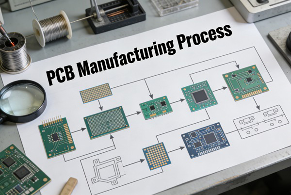
نظرة عامة على عملية تصنيع ثنائي الفينيل متعدد الكلور
على الرغم من أن تعقيد لوحات الدوائر المطبوعة يمكن أن يختلف، إلا أن معظم لوحات الدوائر المطبوعة الصلبة تتبع نفس مسار التصنيع الأساسي:
- تصنيع الطبقة الداخلية
- محاذاة الطبقات والتصفيح
- الحفر
- طلاء النحاس
- تصوير الطبقة الخارجية والحفر
- تطبيق قناع اللحام
- تشطيب السطح
- الطباعة بالشاشة الحريرية
- الاختبار الكهربائي والفحص النهائي
كل خطوة تؤثر بشكل مباشر على الجودة والإنتاجية و التكلفة.
الخطوة 1 - تصنيع الطبقة الداخلية
تصوير الطبقة الداخلية
يبدأ التصنيع بألواح مغلفة بالنحاس. يتم نقل نمط الدائرة المطلوب إلى سطح النحاس باستخدام مادة حساسة للضوء وتعريضها للأشعة فوق البنفسجية.
العوامل الرئيسية:
- دقة عرض التتبع والمسافة بين الخطوط
- دقة محاذاة الصور
- بيئة غرفة نظيفة
حفر الطبقة الداخلية
يتم إزالة النحاس غير المرغوب فيه كيميائياً، تاركاً آثار الدوائر المطلوبة.
من منظور التصنيع:
- تزيد الآثار الدقيقة من صعوبة الحفر
- يؤثر الحفر الزائد أو الحفر الناقص على العائد
في TOPFAST، يتم تحسين معلمات حفر الطبقة الداخلية لتحقيق التوازن الدقة واستقرار الإنتاج.
الخطوة 2 - محاذاة الطبقات وتصفيحها
بالنسبة للوحات الدوائر المطبوعة متعددة الطبقات، يتم تكديس الطبقات الداخلية باستخدام رقائق معدنية مسبقة التشكيل ورقائق نحاسية خارجية.
عملية التصفيح
- الحرارة والضغط يربطان جميع الطبقات معًا
- يضمن المحاذاة الدقيقة اتصالات دقيقة عبر
التأثير على التكلفة والجودة:
- زيادة الطبقات يزيد من دورات التصفيح
- التصفيح المتسلسل يزيد من التعقيد والتكلفة
الخطوة 3 - الحفر
يؤدي الحفر إلى إنشاء ثقوب للوصلات والموصلات المكونة.
الحفر الميكانيكي
يستخدم في:
- ثقوب عبور
- أحجام ثقوب أكبر
تزداد تكلفة الحفر مع:
- أقطار ثقوب أصغر
- نسب عرض إلى ارتفاع أعلى
- عدد الحفر المرتفع
الحفر بالليزر (لوحات الدوائر المطبوعة المتقدمة)
يستخدم الحفر بالليزر في:
- الميكروفيات في لوحات الدوائر المطبوعة HDI
تتطلب هذه العملية معدات متخصصة وتزيد من تكلفة التصنيع.
الخطوة 4 - طلاء النحاس
بعد الحفر، يجب أن تكون الثقوب موصلة للكهرباء.
ترسيب النحاس غير الكهربائي
يتم ترسيب طبقة رقيقة من النحاس داخل الثقوب المحفورة لتمكين الاتصال الكهربائي بين الطبقات.
الطلاء الكهربائي
يتم طلاء النحاس الإضافي على:
- تقوية الثقوب
- تحقيق السماكة المطلوبة للنحاس
يؤثر توحيد الطلاء بشكل مباشر على الموثوقية، خاصة في التطبيقات عالية التيار أو عالية الموثوقية.
الخطوة 5 - تصوير الطبقة الخارجية والنقش على الطبقة الخارجية
يتم تشكيل نمط الدائرة الكهربائية للطبقة الخارجية باستخدام عملية مشابهة للطبقات الداخلية.
التحديات الرئيسية:
- الحفاظ على دقة التتبع بعد الطلاء
- التحكم في سماكة النحاس
- منع القصر أو الفتح
تؤثر معالجة الطبقة الخارجية بشكل كبير على العائد النهائي.
الخطوة 6 - تطبيق قناع اللحام
الغرض من قناع اللحام
قناع اللحام:
- يحمي آثار النحاس
- يمنع انسداد اللحام
- يحسن العزل الكهربائي
تشمل الألوان الشائعة الأخضر والأسود والأزرق والأحمر. ويظل اللون الأخضر هو الخيار الأكثر فعالية من حيث التكلفة والأكثر استخدامًا.
عوامل جودة قناع اللحام
- دقة التسجيل
- سمك القناع
- تعريف الافتتاح
قد تؤدي جودة قناع اللحام الرديئة إلى حدوث عيوب في التجميع لاحقًا.
الخطوة 7 - تشطيب السطح
تحمي طبقة التشطيب السطحية الوسادات النحاسية المكشوفة وتضمن قابلية اللحام.
خيارات تشطيب الأسطح الشائعة
- HASL: فعالة من حيث التكلفة، واسعة الاستخدام
- ENIG: سطح مستوٍ، موثوقية أعلى
- OSP: تكلفة منخفضة، مدة صلاحية محدودة
توصي TOPFAST بلمسات نهائية للأسطح بناءً على متطلبات التطبيق بدلاً من التفضيلات الافتراضية.
الخطوة 8 - الطباعة بالشاشة الحريرية
تضيف الطباعة الحريرية:
- مؤشرات مرجعية للمكونات
- علامات القطبية
- الشعارات أو المعرفات
على الرغم من عدم عملها كهربائياً، إلا أن الشاشة الحريرية الشفافة تحسن دقة التجميع والصيانة.
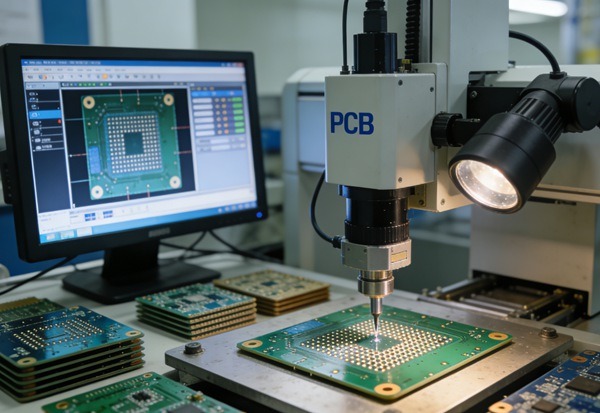
الخطوة 9 - الاختبار الكهربائي والفحص النهائي
الاختبارات الكهربائية
يتم التحقق من خلال الاختبارات الكهربائية مما يلي:
- الاستمرارية
- العزلة
- عدم وجود شورتات وملابس مفتوحة
هذه الخطوة ضرورية لضمان الموثوقية الوظيفية.
الفحص النهائي للجودة
قد تشمل الفحص النهائي ما يلي:
- الفحص البصري
- الهيئة العربية للتصنيع (الفحص البصري الآلي)
- فحوصات الأبعاد
في TOPFAST، تتوافق معايير الفحص مع متطلبات IPC ومواصفات العملاء.
كيف تؤثر عملية تصنيع ثنائي الفينيل متعدد الكلور على التكلفة والجودة
تقدم كل خطوة من خطوات التصنيع ما يلي:
- تقلب العملية
- اعتبارات العائد
- الآثار المترتبة على التكاليف
تشمل العوامل المشتركة المؤثرة على التكلفة ما يلي:
- عدد طبقات مرتفع
- أحجام مثاقب صغيرة
- التفاوتات الضيقة
- تشطيبات سطحية متطورة
فهم العملية برمتها يتيح للمصممين تحسين تصميمات PCB من حيث التكلفة وقابلية التصنيع.
وجهة نظر المُصنِّع: كيف تعمل TOPFAST على تحسين تصنيع ثنائي الفينيل متعدد الكلور
بصفتها شركة مصنعة للوحات الدوائر المطبوعة، تركز TOPFAST على:
- توحيد العمليات
- ردود الفعل المبكرة على DFM
- اتخاذ القرارات على أساس العائد
- إنتاج مستقر وقابل للتطوير
بدلاً من الدفع بعمليات متقدمة غير ضرورية، تركز TOPFAST على تصميمات ملائمة للتصنيع توفر جودة متسقة.
الخاتمة
إن عملية تصنيع ثنائي الفينيل متعدد الكلور عبارة عن سلسلة من الخطوات التي يتم التحكم فيها بعناية، ويساهم كل منها في أداء اللوحة النهائية وموثوقيتها وتكلفتها.
من خلال فهم كيفية تصنيع مركبات ثنائي الفينيل متعدد الكلور - بدءًا من تصنيع الطبقة الداخلية إلى الفحص النهائي - يمكن للمهندسين والمشترين اتخاذ قرارات أفضل في التصميم والتوريد.
مع نهج يركز على التصنيع أولاً، تساعد TOPFAST العملاء على تحويل التصميمات المعقدة إلى لوحات دوائر مطبوعة موثوقة وفعالة من حيث التكلفة.
الأسئلة الشائعة حول عملية تصنيع ثنائي الفينيل متعدد الكلور خطوة بخطوة
ج: يستغرق التصنيع القياسي لثنائي الفينيل متعدد الكلور عادةً من 5 إلى 10 أيام عمل، حسب درجة التعقيد والكمية.
ج: كل خطوة مهمة، لكن الحفر والطلاء مهمان للغاية لضمان الموثوقية الكهربائية.
ج: نعم. تتطلب لوحات الدوائر المطبوعة متعددة الطبقات خطوات إضافية للتصفيح والمحاذاة.
ج: نعم. التصميمات المتوافقة مع قدرات التصنيع تحسن العائد وتقلل التكلفة.
ج: تستخدم TOPFAST عمليات موحدة ومراجعة DFM وفحص شامل لضمان جودة متسقة.