Piirilevyjen tarkastus ja testaus ovat olennaisia vaiheita sen varmistamisessa, että piirilevy täyttää sekä laatu- että toiminnalliset vaatimukset.
Vaikka tarkastuksissa keskitytään vikojen havaitseminen, testaus todentaa sähköinen eheys ja suorituskyky.
Yhdessä ne muodostavat lopullisen laatuportin ennen PCB-kokoonpanoa tai lähetystä.
Tällä sivulla on yleiskatsaus tärkeimpiin piirilevyjen tarkastus- ja testausmenetelmiin ja linkkejä kunkin menetelmän perusteellisiin teknisiin artikkeleihin.
Laadukas perusta:
PCB Quality & Reliability selitetty
Sisällysluettelo
Miksi PCB:n tarkastuksella ja testauksella on merkitystä
Vaikka valmistusprosessit ovat vakaita, vikoja voi silti esiintyä.
Tarkastus ja testaus auttavat:
- Havaitse valmistusvirheet varhaisessa vaiheessa
- Estä viallisia levyjä pääsemästä kokoonpanoon
- Palautteen antaminen prosessin parantamista varten
- Vähentää luotettavuus- ja kenttävikariskiä
Ne eivät korvaa hyvää suunnittelua tai prosessinvalvontaa, mutta ne vähentävät riskiä merkittävästi.
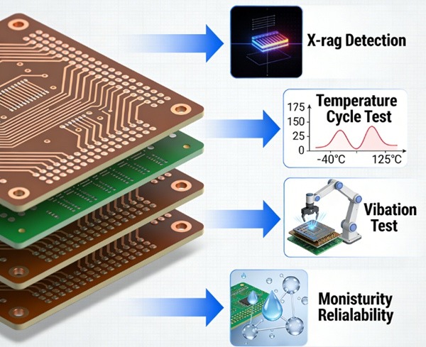
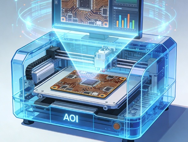
Automaattinen optinen tarkastus (AOI)
AOI on PCB-valmistuksessa yleisimmin käytetty tarkastusmenetelmä.
Mitä AOI tekee hyvin
- Havaitsee pintatason viat
- Tunnistaa aukkojen ja oikosulkujen muodot visuaalisesti
- Parantaa tarkastuksen nopeutta ja johdonmukaisuutta
AOI-rajoitukset
- Sisäisiä vikoja ei voida havaita
- Sähköistä suorituskykyä ei voida todentaa
Syväsukellus:
AOI-tarkastus PCB-valmistuksessa
Röntgentarkastus
Röntgentarkastus mahdollistaa näkyvyyden piirilevyn sisäisiin rakenteisiin.
Mitä röntgen havaitsee
- Läpiviennit ja reikien pinnoitushuokoset
- Sisäisen kerroksen virheasento
- Delaminaatio ja hartsihuokoset
Röntgenkuvauksen rajoitukset
- Korkeammat kustannukset
- Hitaampi tarkastusnopeus
- Tyypillisesti näytteenottoon perustuva
Tekniset tiedot:
Röntgentarkastus PCB-valmistuksessa
PCB:n sähköinen testaus
Sähköinen testaus on ainoa menetelmä, jolla liitettävyys voidaan todentaa suoraan.
Mitä sähkötestaus vahvistaa
- Kaikkien verkkojen jatkuvuus
- Lyhyiden housujen puuttuminen
- Oikeat verkkoyhteydet
Mitä se ei voi tehdä
- Ennustaa pitkän aikavälin luotettavuutta
- Sisäisten onteloiden tai pinnoitepaksuuden havaitseminen
Menetelmän yleiskatsaus:
PCB:n sähköinen testaus selitetty
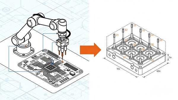
Lentävä koetin vs. kiinnitykseen perustuva testaus
Kun sähkötestausta tarvitaan, oikean menetelmän valinta on ratkaisevan tärkeää.
Keskeiset päätöstekijät
- Tuotannon määrä
- Suunnittelun vakaus
- Kustannusrakenne
- Time-to-market
Vertailuopas:
Lentävä koetin vs. kiinnityslaitteen sähköinen testaus
Tarkastus vs. testaus - eron ymmärtäminen
| Aspect | Tarkastus | Testaus |
|---|---|---|
| Focus | Visuaalinen ja rakenteellinen | Sähköinen toiminta |
| Tyypilliset menetelmät | AOI, röntgen | E-Test |
| Havaitsee aukot/lyhyet kohdat | Rajoitettu | Kyllä |
| Havaitsee sisäiset viat | Vain röntgenkuvaus | No |
| Luotettavuuden ennuste | No | No |
Molemmat ovat välttämättömiä, mutta ne kohdistuvat eri riskeihin.
Miten tarkastus ja testaus toimivat yhdessä
Täydellinen piirilevyjen laatujärjestelmä noudattaa tyypillisesti tätä järjestystä:
- AOI pinnan vikojen varhaiseen havaitsemiseen
- sisäisten rakenteiden röntgentarkastus (tarvittaessa)
- Sähköinen testaus liitettävyyden tarkistamiseksi
- Luotettavuuden testaus pitkän aikavälin suorituskykyä varten (valikoiva)
Luotettavuuslinkki:
PCB-luotettavuuden testaus selitetty
Kustannusnäkökohdat tarkastuksessa ja testauksessa
Tarkastus ja testaus lisäävät kustannuksia, mutta niiden ohittaminen lisää riskiä.
Kustannuksiin vaikuttavat:
- Hallituksen monimutkaisuus
- Volume
- Tarkastussyvyys
- Testimenetelmän valinta
Kustannustasapaino:
PCB-valmistuksen kustannukset vs. laatu Trade-offs
Milloin tehostettu tarkastus on tarpeen
Tehostettu tarkastus ja testaus ovat erityisen tärkeitä seuraavissa tapauksissa:
- Suuritiheyksiset tai monikerroksiset piirilevyt
- Uudet mallit tai materiaalit
- Korkean jännitteen tai korkean lämpötilan sovellukset
- Pitkän käyttöiän tuotteet
Tällaisissa tapauksissa pelkkä tavanomainen tarkastus ei riitä.
Tällaisissa tapauksissa pelkkä tavanomainen tarkastus ei riitä.
Miten valmistajat soveltavat tarkastusta käytännössä
Todellisissa tuotantoympäristöissä tarkastusstrategiat räätälöidään seuraaviin seikkoihin:
- Suunnitteluriski
- Volyymin taloustiede
- Asiakkaan vaatimukset
TOPFASTissa tarkastus- ja testausmenetelmät valitaan seuraavien seikkojen perusteella riskitaso ja sovellustarpeet, mikä takaa sekä tehokkuuden että luotettavuuden.
Päätelmä
Piirilevyjen tarkastus ja testaus ovat olennaisia suojatoimia, jotka muodostavat sillan valmistusprosessien ja todellisen maailman suorituskyvyn välille.
Yhdistämällä AOI, röntgentarkastus, sähköinen testaus ja asianmukaiset testausstrategiat valmistajat voivat merkittävästi vähentää vikariskiä ja parantaa piirilevyjen kokonaislaatua.
Tämä sivu toimii keskeisenä viitekehyksenä seuraaville PCB:n tarkastus ja testaus aihepiiriklusteri.
PCB Inspection & Testing FAQ
V: Ei. Tarkastus ei voi todentaa sähköistä liitettävyyttä.
V: Ei. Ne havaitsevat erityyppisiä vikoja.
V: Ei. Röntgensäteilyä käytetään yleensä monimutkaisissa malleissa.
V: Ei. Luotettavuustestaus on tarpeen pitkän aikavälin validointia varten.
V: Ainoastaan matalan riskin ja vähäisen monimutkaisuuden sovelluksissa.