Проверка и тестирование печатных плат - важнейшие этапы обеспечения соответствия печатной платы требованиям к качеству и функциональности.
В то время как инспекция сосредоточена на обнаружение дефектов, тестирование проверяет электрическая целостность и производительность.
Вместе они образуют окончательный контроль качества перед сборкой или отгрузкой печатной платы.
На этой странице представлен обзор наиболее важных методов проверки и тестирования печатных плат, а также ссылки на подробные технические статьи по каждому из них.
Качественная основа:
Качество и надежность печатных плат: объяснение
Ii. Содержание
Почему проверка и тестирование печатных плат имеют значение
Даже при надежных производственных процессах все равно возможны дефекты.
Проверка и тестирование помогают:
- Выявляйте производственные ошибки на ранней стадии
- Предотвращение попадания дефектных плат в сборку
- Предоставление обратной связи для улучшения процесса
- Снижение надежности и риска отказов в полевых условиях
Они не заменяют качественное проектирование или контроль процесса, но значительно снижают риск.
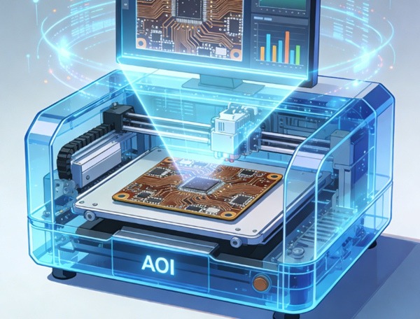
Автоматизированный оптический контроль (AOI)
AOI - наиболее часто используемый метод контроля при производстве печатных плат.
Что AOI делает хорошо
- Обнаружение дефектов на уровне поверхности
- Визуально определяет обрывы и замыкания
- Повышает скорость и последовательность проверки
Ограничения AOI
- Невозможно обнаружить внутренние дефекты
- Невозможно проверить электрические характеристики
Глубокое погружение:
Контроль AOI при производстве печатных плат
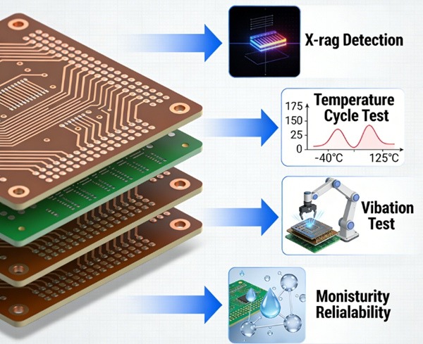
Рентгеновский контроль
Рентгеновский контроль позволяет увидеть внутренние структуры печатной платы.
Что обнаруживает рентген
- Пустоты в отверстиях и покрытиях
- Перекос внутреннего слоя
- Расслоение и пустоты в смоле
Ограничения рентгена
- Более высокая стоимость
- Замедление скорости осмотра
- Как правило, на основе выборки
Технические детали:
Рентгеновский контроль при производстве печатных плат
Электрические испытания печатных плат
Электрические испытания - это единственный метод, позволяющий напрямую проверить надежность соединения.
Что подтверждают электрические испытания
- Непрерывность всех сетей
- Отсутствие шорт
- Правильное подключение к сети
Что он не может сделать
- Прогнозирование долгосрочной надежности
- Обнаружение внутренних пустот или толщины покрытия
Обзор метода:
Электрические испытания печатных плат Объяснения
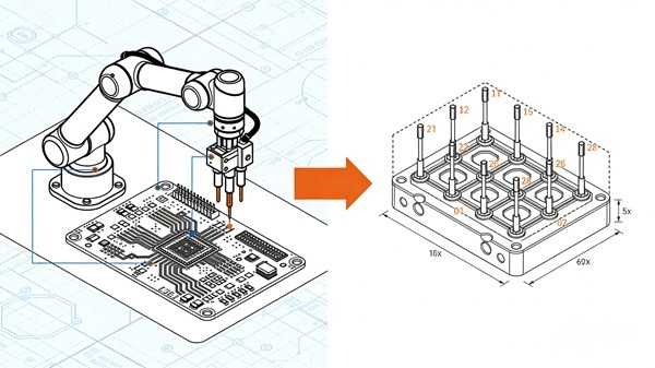
Летающий зонд в сравнении с испытаниями на основе приспособлений
При необходимости проведения электрических испытаний выбор правильного метода становится критически важным.
Ключевые факторы принятия решений
- Объем производства
- Стабильность конструкции
- Структура затрат
- Время выхода на рынок
Руководство по сравнению:
Электрические испытания с помощью летающего зонда и приспособления
Инспекция и тестирование - понимание разницы
| Аспект | Инспекция | 3. Испытание |
|---|---|---|
| В центре внимания | Визуальный и структурный | Электрическая функция |
| Типичные методы | AOI, рентген | E-Test |
| Обнаружение обрывов/коротких замыканий | Ограниченный | Да |
| Обнаружение внутренних дефектов | Только рентген | Нет |
| Прогнозирование надежности | Нет | Нет |
Оба варианта необходимы, но они направлены на борьбу с разными рисками.
Как инспекция и тестирование работают вместе
Полная система качества печатных плат обычно строится в такой последовательности:
- AOI для раннего обнаружения дефектов поверхности
- Рентгеновский контроль внутренних структур (при необходимости)
- Электрические испытания для проверки возможности подключения
- Проверка надежности для обеспечения долгосрочной работы (выборочно)
Ссылка на надежность:
Тестирование надежности печатных плат: объяснение
Учет затрат при проведении инспекций и испытаний
Инспекция и тестирование увеличивают стоимость, но их пропуск повышает риск.
На стоимость влияют:
- Сложность управления
- В Том числе:
- Глубина осмотра
- Выбор метода испытания
Баланс затрат:
Компромиссы между стоимостью и качеством при производстве печатных плат
Когда необходимо проводить расширенный осмотр
Усиленная проверка и тестирование особенно важны для:
- Высокоплотные или многослойные печатные платы
- Новые конструкции или материалы
- Высоковольтные или высокотемпературные приложения
- Продукты с длительным сроком службы
В таких случаях одного стандартного осмотра недостаточно.
В таких случаях одного стандартного осмотра недостаточно.
Как производители применяют инспекцию на практике
В реальных производственных условиях стратегии инспекции разрабатываются с учетом:
- Риск при проектировании
- Объемная экономика
- Требования заказчика
В компании TOPFAST методы контроля и испытаний выбираются на основе уровень риска и потребности приложенияобеспечивая эффективность и надежность.
Iii. Выводы и рекомендации
Проверка и тестирование печатных плат - важнейшие средства защиты, обеспечивающие связь между производственными процессами и реальными характеристиками.
Комбинируя АОИ, рентгеновский контроль, электрические испытания и соответствующие стратегии тестирования, производители могут значительно снизить риск дефектов и повысить общее качество печатных плат.
Эта центральная страница служит центральным справочником для Инспекция и тестирование печатных плат тематический кластер.
FAQ по проверке и тестированию печатных плат
О: Нет. Осмотр не позволяет проверить электрическое подключение.
О: Нет. Они обнаруживают разные типы дефектов.
О: Нет. Рентген обычно используется для сложных конструкций.
О: Нет. Испытания на надежность необходимы для долгосрочной проверки.
О: Только для приложений с низким уровнем риска и низкой сложностью.