كيف يتم تحديد عدد طبقات ثنائي الفينيل متعدد الكلور بشكل علمي؟
جدول المحتويات
المفاهيم الأساسية وأهمية تعداد طبقات ثنائي الفينيل متعدد الكلور
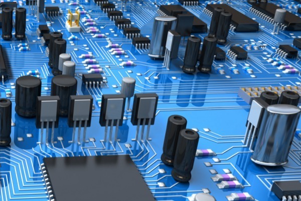
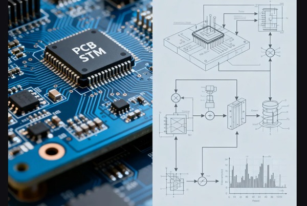
تُعد مركبات ثنائي الفينيل متعدد الكلور من المكونات الأساسية للأجهزة الإلكترونية الحديثة، ويؤثر اختيار عدد الطبقات بشكل مباشر على أداء المنتج وموثوقيته وتكلفته. مع ازدياد تعقيد الأجهزة الإلكترونية، ظهرت مركبات ثنائي الفينيل متعدد الكلور متعددة الطبقات (عادةً ما تكون مكونة من 4 طبقات أو 6 طبقات أو 8 طبقات أو أكثر) لتلبية متطلبات التصميم الأكثر تعقيدًا عن طريق إضافة طبقات موصلة إضافية داخليًا.
لماذا تكون طبقات ثنائي الفينيل متعدد الكلور دائماً أرقام زوجية؟
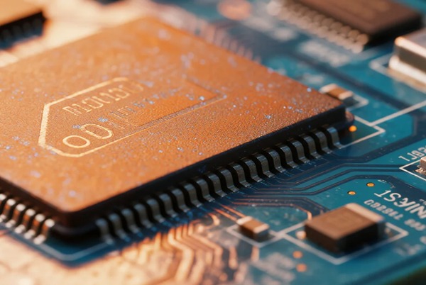
ونظرًا لأن عملية التصنيع تتطلب تصفيح رقائق النحاس في أزواج، فإن تقنية ثنائي الفينيل متعدد الكلور الحديثة المتطورة تسمح حتى بتضمين المكونات في الطبقات الداخلية لثنائي الفينيل متعدد الكلور.يعزز هذا التصميم المبتكر من تكامل الدوائر والأداء.
تأثير عدد طبقات ثنائي الفينيل متعدد الكلور على أداء المنتج
- الأداء الكهربائي: المزيد من الطبقات يعني تكاملاً أفضل للإشارة والتوافق الكهرومغناطيسي.
- كثافة التوجيهتتطلب الدوائر المعقدة المزيد من الطبقات للتوصيلات البينية.
- هيكل التكلفة: تؤدي زيادة عدد الطبقات إلى رفع تكاليف التصنيع بشكل كبير.
من الإلكترونيات الاستهلاكية إلى المعدات الفضائية، تختلف مجالات التطبيقات المختلفة اختلافًا كبيرًا في متطلبات عدد طبقات ثنائي الفينيل متعدد الكلور.يمكن أن يفي التصميم المعقول للطبقات بمتطلبات الأداء مع التحكم في التكاليف، ولكن يمكن أن يؤدي الاختيار الخاطئ إلى فشل المنتج أو تصاعد التكلفة. على سبيل المثال، قد لا تتطلب الآلة الحاسبة البسيطة سوى ثنائي الفينيل متعدد الكلور من طبقة واحدة فقط، بينما تستخدم الهواتف الذكية عادةً 8-10 طبقات، وقد تصل اللوحات الأم للخوادم عالية الأداء إلى 16 طبقة أو أكثر.
العوامل الرئيسية في تحديد عدد طبقات ثنائي الفينيل متعدد الكلور
إن اختيار عدد طبقات ثنائي الفينيل متعدد الكلور هو عملية صنع قرار تتطلب دراسة شاملة لعوامل متعددة.عندما يرغب العملاء في تصنيع ألواح ثنائي الفينيل متعدد الكلور، يحتاج المصنعون إلى فهم واضح لمتطلبات المستخدمين&8217؛ وتقديم توصيات مقابلة من المهندسين لإيجاد التوازن الأمثل بين متطلبات الأداء وقيود التكلفة، وبالتالي تزويد العملاء بمنتجات مرضية وخدمة ممتازة.
متطلبات مجال التطبيق وتردد التشغيل
الأجهزة الإلكترونية في الصناعات المختلفة لها متطلبات مختلفة إلى حد كبير لمركبات ثنائي الفينيل متعدد الكلور. تردد التشغيل هي إحدى المعلمات الأساسية التي تحدد عدد طبقات ثنائي الفينيل متعدد الكلور، حيث تتطلب التطبيقات عالية التردد عادةً المزيد من الطبقات لضمان سلامة الإشارة. على سبيل المثال:
- الإلكترونيات الاستهلاكية (مثل سماعات البلوتوث):عادةً ما تكون الألواح من 4-6 طبقات
- معدات الاتصالات السلكية واللاسلكية (على سبيل المثال، المحطات القاعدية للجيل الخامس 5G):قد تتطلب 12 طبقة أو أكثر
- إلكترونيات السيارات (مثل وحدات التحكم بوحدة التحكم بوحدة التحكم الإلكترونية):6-8 طبقات بشكل أساسي
- أنظمة الفضاء الجوي:10 طبقات أو أكثر لضمان موثوقية عالية للغاية
تتسم الدوائر عالية التردد (120 ميجا هرتز) بمتطلبات أكثر صرامة فيما يتعلق بعدد طبقات ثنائي الفينيل متعدد الكلور لأن زيادة سرعات نقل الإشارة تجلب مخاطر تداخل كهرومغناطيسي أكبر (EMI).وتوفر مركبات ثنائي الفينيل متعدد الكلور متعددة الطبقات مستويات طاقة وأرضية مخصصة، مما يتحكم بفعالية في مسارات عودة الإشارة ويقلل من الحديث المتبادل والإشعاع.
تعقيد الدائرة وتقييم كثافة المكونات
تعقيد الدائرة يؤثر بشكل مباشر على متطلبات عدد طبقات ثنائي الفينيل متعدد الكلور. يمكن تقييم التعقيد من الأبعاد التالية:
- عدد المكونات:خاصة الأجهزة ذات العدد الكبير من السنون مثل حزم BGA
- عدد شبكات الإشارة:إجمالي الوصلات البينية المطلوبة
- متطلبات التصميم الخاصة:مثل التحكم في المعاوقة والأزواج التفاضلية ومطابقة الطول
كثافة المكونات هو مقياس مهم آخر، يمكن حسابه من خلال معادلة كثافة رقم التعريف الشخصي:
كثافة الدبابيس = مساحة اللوحة (بالم²) / (إجمالي عدد الدبابيس على اللوحة/14)بناءً على نتائج الحساب، يمكن الرجوع إلى القيم التجريبية التالية:
- وضع المكون من جانب واحد: كثافة PIN> 1.0 قد تستخدم طبقتين؛ 0.6-1.0 تقترح 4 طبقات؛ <؛ 0.6 تتطلب 6 طبقات أو أكثر
- وضع المكونات على الوجهين:يمكن تخفيف معايير الكثافة ولكن يجب مراعاة عوامل تبديد الحرارة وعوامل التجميع
اعتبارات الميزانية والجدول الزمني للتصنيع
عند النظر في عدد طبقات ثنائي الفينيل متعدد الكلور، فإن تكلفة التصنيع عامل لا يمكن تجاهله.ويكمن الفرق في التكلفة بين مركبات ثنائي الفينيل متعدد الكلور أحادية/مزدوجة الطبقة ومتعددة الطبقات بشكل أساسي في تعقيد التصميم والتصنيع. غالبًا ما تأتي السعة الأعلى بتكلفة أعلى.
وعلاوة على ذلك، هناك علاقة تناسبية بين عدد طبقات ثنائي الفينيل متعدد الكلور والسعر - وبشكل عام، يعني المزيد من الطبقات ارتفاع الأسعار.ويرجع ذلك في المقام الأول إلى أن تصميم ثنائي الفينيل متعدد الكلور متعدد الطبقات وعمليات التصنيع أكثر تعقيدًا، مما يزيد التكاليف بطبيعة الحال.لتقييم تكاليف ثنائي الفينيل متعدد الكلور بشكل أكثر دقة، يمكنك استخدام مواقع الويب الخاصة بعرض أسعار ثنائي الفينيل متعدد الكلور التي تساعد في تقدير التكاليف بناءً على معايير مختلفة مثل نوع الموصل والحجم والكمية وعدد الطبقات. يمكن أن تساعد الآلات الحاسبة عبر الإنترنت أيضًا في تحديد مواد العزل والسماكات المناسبة لفهم أكثر شمولاً لهياكل تكاليف ثنائي الفينيل متعدد الكلور.
وقت التسليم هو عامل حاسم آخر في تصنيع ثنائي الفينيل متعدد الكلور، خاصةً بالنسبة للإنتاج بكميات كبيرة. تختلف أوقات التسليم حسب عدد الطبقات، ويعتمد ذلك بشكل أساسي على مساحة ثنائي الفينيل متعدد الكلور. يمكن لزيادة الاستثمار في بعض الأحيان تقصير أوقات التسليم.
كثافة الدبوس ومتطلبات طبقة الإشارة
كما يرتبط اختيار عدد طبقات ثنائي الفينيل متعدد الكلور ارتباطاً وثيقاً بكثافة الدبوس واحتياجات طبقة الإشارة.على سبيل المثال، عادةً ما تتطلب كثافة الدبابيس التي تبلغ 0 طبقة إشارة طبقتين، بينما تتطلب كثافة الدبابيس الأقل طبقات أكثر.عندما تصل كثافة الدبوس إلى 2 أو أقل، قد تكون هناك حاجة إلى 10 طبقات على الأقل.
طريقة اختيار طبقة ثنائي الفينيل متعدد الكلور
في التصميم الهندسي الفعلي، يتطلب اختيار أرقام طبقات ثنائي الفينيل متعدد الكلور اتخاذ قرارات علمية بناءً على متطلبات المشروع المحددة والقيود الفنية.فيما يلي الطرق العملية والقواعد الأساسية التي لخصتها Topfast استنادًا إلى أكثر من عشر سنوات من الخبرة في تصنيع ثنائي الفينيل متعدد الكلور.
تقدير عدد الطبقات بناءً على كثافة الدبوس
كثافة الدبوس مقياسًا فعالاً لتقييم متطلبات عدد طبقات ثنائي الفينيل متعدد الكلور محسوبًا على النحو التالي
كثافة المسامير = مساحة اللوحة (بالم²) / (إجمالي عدد المسامير على اللوحة/14)بناءً على النتائج، راجع معايير الاختيار التالية:
الجدول: كثافة الدبوس مقابل عدد الطبقات لوضع المكونات أحادية الجانب
| نطاق كثافة الدبوس | الطبقات الموصى بها | التطبيقات |
|---|---|---|
| >1.0 | 2 | الإلكترونيات الاستهلاكية البسيطة |
| 0.7-1.0 | 4 | الضوابط الصناعية العامة |
| 0.5-0.7 | 6 | معدات الشبكات |
| 0.5؛ 0.5 | 8+ | الخوادم المتطورة |
الجدول: كثافة الدبوس مقابل عدد الطبقات للوضع على الوجهين
| نطاق كثافة الدبوس | الطبقات الموصى بها | التطبيقات |
|---|---|---|
| >1.5 | 2 | منتجات متوسطة ومنخفضة التعقيد |
| 1.0-1.5 | 4 | الأجهزة الطرفية للهواتف الذكية |
| 0.7-1.0 | 6 | إلكترونيات السيارات |
| 0.7؛ 0.7 | 8+ | الحوسبة عالية الأداء |
قواعد التكرار إلى عدد الطبقات في الإبهام
تردد المعالج هو اعتبار رئيسي آخر، حيث تتطلب الدوائر عالية التردد عادةً طبقات أكثر لسلامة الإشارة:
- 50 ميجا هرتز: عادة ما تكون كافية مع طبقتين
- 50- 120 ميجا هرتز: يوصى ب 4 طبقات (إشارة-أرضي-طاقة-إشارة-طاقة-إشارة)
- 120 ميجا هرتز - 1 جيجا هرتز:: 6 طبقات (أفضل أداء من حيث التكلفة)
- >1 جيجا هرتز: يتطلب أكثر من 8 طبقات مع تحليل صارم من SI
الحالات الخاصة التي تتطلب المزيد من الطبقات على الرغم من انخفاض الترددات:
- نطاقات جهد متعددة (≥3 مصادر طاقة مستقلة)
- واجهات تسلسلية عالية السرعة (PCIe، USB3.0+)
- دوائر تناظرية حساسة (ADC/DAC عالية الدقة)
استراتيجيات نوع الذاكرة وعدد الطبقات
النظام الفرعي للذاكرة تؤثر الخصائص بشكل كبير على عدد طبقات ثنائي الفينيل متعدد الكلور:
أنظمة الذاكرة الثابتة:
- SRAM/ذاكرة وصول عشوائي SRAM/ذاكرة فلاش NOR المتوازية: قد تكفي طبقتان
- نقطة أساسية: ضمان استقرار الطاقة
أنظمة الذاكرة الديناميكية:
- SDRAM/DDR: 4 طبقات كحد أدنى
- DDR2/3: يوصى بـ 6 طبقات (مع مستويات مرجعية مخصصة)
- DDR4/5: يتطلب أكثر من 8 طبقات مع مطابقة صارمة للطول
أنظمة فلاش NAND:
- تقنية NAND التقليدية: 4 طبقات كافية
- eMMC/UFS: تحدد حسب التردد (عادةً 6 طبقات)
تعبئة وتغليف BGA وتكييف عدد الطبقات
جهاز BGA يؤثر التغليف مباشرة على عدد طبقات ثنائي الفينيل متعدد الكلور:
رمية الدبوس مقابل عدد الطبقات:
- ≥ 1.0 مم: قد تعمل طبقتان
- درجة 0.8 مم: اقتراح 4 طبقات
- 0.65 مم:يوصى بـ 6 طبقات
- ≤0.5 مم:تتطلب أكثر من 8 طبقات
إرشادات عدد الدبابيس:
- <100 دبوس: النظر في عدد أقل من الطبقات
- 100-300 دبابيس 100-300:الطبقات القياسية الموصى بها
- >300 دبوس:إضافة 1-2 طبقات
أنواع BGA الخاصة:
- الرقاقة القلابة BGA: إضافة طبقتين
- BGA متناهية الدقة (≤0.4 مم): تتطلب تقنية HDI
اعتبارات عدد الطبقات الخاصة بالصناعة
الصناعات المختلفة لها متطلبات خاصة تؤثر على عدد الطبقات:
إلكترونيات السيارات:
- الأساسي: 4 طبقات كحد أدنى (الموثوقية)
- مجموعة نقل الحركة: 6 طبقات + مواد عالية الحرارة
- أنظمة ADAS: 8 طبقات + مواد عالية التردد
الأجهزة الطبية:
- معدات التشخيص: 6 طبقات (ضوضاء منخفضة)
- الأجهزة القابلة للزرع:4 طبقات (التصغير)
الضوابط الصناعية:
- PLC قياسي: 4 طبقات
- التحكم في الحركة: 6 طبقات (مقاومة التداخل الكهرومغناطيسي)
الإلكترونيات الاستهلاكية:
- الأجهزة القابلة للارتداء: 4 طبقات (التصغير)
- المنزل الذكي:يختلف حسب الوظيفة
تحسين التكلفة وتسويات عدد الطبقات
تحت ضغط الميزانية، ضع في اعتبارك ما يلي استراتيجيات تحسين عدد الطبقات:
- “Pseudo-multi-layer” design:
- استخدم طبقتين + وصلات عبور لمحاكاة الوظائف متعددة الطبقات
- مناسبة للتصاميم منخفضة التردد ومنخفضة الكثافة
- تقنية التصفيح الهجين:
- زيادة الطبقات محليًا (على سبيل المثال، تحت مناطق BGA)
- يوازن بين التكلفة والأداء
- تكديس الطبقات غير المتماثلة:
- تقليل طبقات الإشارة ولكن مع الحفاظ على مستويات الطاقة/الأرضية
- على سبيل المثال، لوحة من 6 طبقات بتكوين 1-2-2-1
- الاستعاضة عن تكنولوجيا مبادرة التنمية البشرية:
- استخدام وصلات بينية عالية الكثافة لتقليل إجمالي الطبقات
- مثالية للتصميمات ذات العدد الكبير من المسامير ولكن ذات المساحة الصغيرة
من خلال النظر بشكل شامل في جميع العوامل المذكورة أعلاه إلى جانب متطلبات وقيود المشروع المحددة، يمكن للمهندسين إجراء اختيارات سليمة علميًا لعدد طبقات ثنائي الفينيل متعدد الكلور التي توازن بين الأداء والموثوقية والتكلفة على النحو الأمثل.
الأسئلة الشائعة (FAQ)
في عملية اختيار أرقام طبقات ثنائي الفينيل متعدد الكلور، غالبًا ما تصادف بعض المشاكل والالتباسات النموذجية. يتم توفير إجابات احترافية لهذه الأسئلة الشائعة.
كيف تحدد متى يحتاج التصميم إلى المزيد من طبقات ثنائي الفينيل متعدد الكلور؟
تشير عدة مؤشرات واضحة إلى الحاجة إلى زيادة طبقات ثنائي الفينيل متعدد الكلور:
- إكمال التوجيه غير كافٍ:
- تعذر إكمال التوجيه بعد الوصول إلى 90%
- الاستخدام المكثف لقفزات العبور لحل التداخلات
- مشكلات سلامة الإشارة:
- تُظهر الإشارات الحرجة رنينًا شديدًا
- فشل اختبارات الرسم البياني للعين
- تجاوز معدل خطأ البت في النظام الحدود المسموح بها
- مشاكل استقرار الطاقة:
- تقلبات الجهد الكهربائي تتجاوز حدود التحمل
- ضوضاء التحويل المتزامن الملحوظة (SSN)
- فشل اختبار EMC:
- الانبعاثات المشعة تتجاوز المعايير
- اختبارات المناعة غير ناجحة
- صعوبات الإدارة الحرارية:
- ارتفاع درجة الحرارة المحلية غير قابل للحل مع الطبقات الحالية
- تحتاج إلى طبقات حرارية إضافية أو طبقات حرارية إضافية
طرق التحقق العملية:
- يُظهر فحص قواعد التصميم (DRC) العديد من الانتهاكات
- عرض ثلاثي الأبعاد يكشف عن توجيه مزدحم للغاية
- يشير تحليل المحاكاة إلى عدم استيفاء المعلمات الحرجة
ما المشكلات المحتملة التي تنشأ من زيادة طبقات ثنائي الفينيل متعدد الكلور؟
في حين أن إضافة الطبقات تحل العديد من تحديات التصميم، إلا أنها قد تقدم ما يلي مشاكل جديدة:
- الزيادات في التكلفة:
- زيادة التكلفة بنسبة 30-50% لكل طبقتين إضافيتين
- ارتفاع النفقات الهندسية غير المتكررة (NRE)
- انخفاض عوائد الإنتاج:
- زيادة الصعوبة في محاذاة الطبقات
- ارتفاع معدلات عيوب الطبقة الداخلية
- المهل الزمنية الممتدة:
- 3-5 أيام إضافية لكل طبقتين إضافيتين
- خيارات محدودة للتعجيل العاجل
- صعوبات الإصلاح:
- من الصعب اكتشاف عيوب الطبقة الداخلية
- انخفاض معدلات نجاح إعادة العمل
- زيادة الوزن والسمك:
- تصميمات الأجهزة المحمولة المؤثرة
- قد يتجاوز الحدود الميكانيكية
استراتيجيات التخفيف من المخاطر:
- استخدام تصاميم الطبقات المتدرجة (اختلاف عدد الطبقات حسب المساحة)
- اعتماد HDI لتقليل متطلبات الطبقة الكلية
- تحسين التراكمات لتحسين الإنتاجية
كيف توازن بين التكلفة والأداء لتحقيق العدد الأمثل للطبقات؟
طرق الموازنة بين التكلفة والأداء:
- نهج التحقق التدريجي:
- بدء النماذج الأولية بطبقات أقل
- قرر ما إذا كنت تريد إضافة طبقات بناءً على نتائج الاختبار أم لا
- تحليل المسار الحرج:
- تحديد مسارات الإشارات الأكثر أهمية
- إضافة طبقات لهذه الأقسام فقط
- مصفوفة تقييم التكلفة والعائد:
| خيار الطبقة | نقاط الأداء | نقاط التكلفة | القيمة المركبة |
|---|---|---|---|
| 4 طبقات | 70 | 90 | 78 |
| 6 طبقات | 85 | 70 | 80 |
| 8 طبقات | 95 | 50 | 75 |
- نهج التصميم المعياري:
- الوحدات الأساسية تستخدم وحدات أساسية متعددة الطبقات
- تستخدم الدوائر الطرفية طبقة من طبقتين
القواعد الأساسية العملية:
- المنتجات الاستهلاكية: ≤6 طبقات
- معدات صناعية: 4-8 طبقات مثالية
- معدات الربط الشبكي: 6-12 طبقة شائعة
- حوسبة متطورة أكثر من 12 طبقة
ما هي التطبيقات النموذجية لمختلف طبقات ثنائي الفينيل متعدد الكلور؟
التطبيقات المميزة حسب عدد الطبقات
2-طبقة 2:
- لوحات التحكم في الأجهزة
- دوائر الطاقة البسيطة
- الوحدات الصناعية الأساسية
- الألعاب الإلكترونية
4 طبقات:
- الهواتف الذكية
- الموجهات
- وحدات التحكم الإلكتروني في السيارات
- الشاشات الطبية
6 طبقات:
- بطاقات الرسومات المتطورة
- أجهزة التحكم المنطقي القابلة للبرمجة القابلة للبرمجة الصناعية
- مفاتيح تبديل الشبكة
- وحدات التحكم في الطائرات بدون طيار
8 طبقات:
- اللوحات الأم للخوادم
- محطات الجيل الخامس 5G القاعدية
- نظام مساعدة السائق الآلي المتطور
- أدوات اختبار متميزة
10+ طبقة:
- الحواسيب الفائقة
- إلكترونيات الفضاء الجوي
- أنظمة الرادار المتطورة
- لوحات خلفية معقدة
المفاهيم الخاطئة الشائعة في اختيار عدد طبقات ثنائي الفينيل متعدد الكلور
- “المزيد من الطبقات أفضل دائمًا”.:
- الحقيقة: الإفراط في الهندسة الهندسية يهدر التكاليف
- الحقيقة: تلبية المتطلبات بشكل كافٍ
- “لا يمكن لطبقتين&8217;أن تعمل بسرعة عالية&8221;”عالية السرعة;:
- حقيقة: الدوائر البسيطة عالية السرعة ممكنة
- الحقيقة: يتطلب تصميمًا دقيقًا
- “يجب أن تكون طائرات الطاقة صلبة”:
- حقيقة: قد تكون الطائرات المنقسمة أفضل
- الحقيقة: يعتمد على الاحتياجات الحالية
- “إشارات الطبقة الداخلية أضعف”:
- حقيقة: الإشارات الداخلية أكثر استقرارًا
- الحقيقة: تتأثر بالطائرات المرجعية
- “إضافة طبقات تحل دائمًا مشكلة EMC.”:
- حقيقة: يمكن أن يؤدي سوء التكدس إلى تفاقم التوافق الكهرومغناطيسي EMC
- الحقيقة: التصميم المكدس أكثر أهمية
الممارسات الصحيحة:
- اتخاذ القرارات على أساس متطلبات النظام
- التحقق من الصحة من خلال المحاكاة
- استشر الشركة المصنعة للوحات ثنائي الفينيل متعدد الكلور&8217;استشارة الشركة المصنعة للوحات ثنائي الفينيل متعدد الكلور
- تصميمات مرجعية ناجحة مماثلة


منشورات ذات صلة