تصنيع ثنائي الفينيل متعدد الكلور هو عملية متعددة الخطوات ومحكومة بإحكام حيث يمكن أن تؤدي الانحرافات الصغيرة إلى مشاكل في الموثوقية أو فقدان العائد أو زيادة التكلفة.
في حين أن العديد من المصادر تصف تصنيع ثنائي الفينيل متعدد الكلور على مستوى عالٍ، فإن فهم كيف تتفاعل كل خطوة تصنيع مع الخطوة التالية أمر بالغ الأهمية لـ
- تصميم لوحات قابلة للتصنيع
- التحكم في التكلفة
- ضمان الموثوقية على المدى الطويل
يقدم هذا المقال نظرة عامة على عملية تصنيع ثنائي الفينيل متعدد الكلور خطوة بخطوة، مع روابط لشرح متعمق لكل مرحلة من المراحل الحرجة.
يعكس المنظور ممارسات التصنيع الحقيقية التي يستخدمها مصنعو ثنائي الفينيل متعدد الكلور المحترفون مثل توب فاستحيث يكون استقرار العملية والتحكم في الإنتاجية من الأولويات الأساسية.
جدول المحتويات
لمحة عامة عن عملية تصنيع ثنائي الفينيل متعدد الكلور
يتضمن سير العمل النموذجي لتصنيع ثنائي الفينيل متعدد الكلور ما يلي:
- تصنيع الطبقة الداخلية
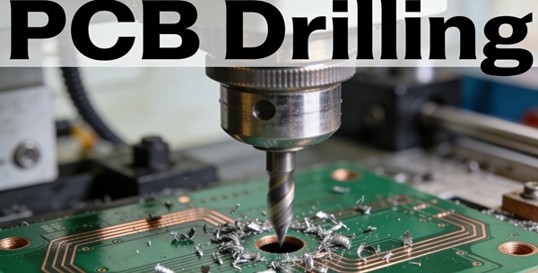
- الحفر (ميكانيكي أو ليزر)
- طلاء النحاس
- نقش النمط المحفور
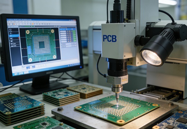
- الفحص ومراقبة المحصول
تعتمد كل خطوة على الخطوة السابقة. وغالباً ما لا يمكن تصحيح الأخطاء في وقت مبكر من العملية في وقت لاحق.
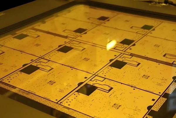
تصنيع الطبقة الداخلية
تصنيع الطبقة الداخلية هو أساس تصنيع ثنائي الفينيل متعدد الكلور متعدد الطبقات.
في هذه المرحلة
- رقائق النحاس منقوشة لتشكيل دوائر داخلية
- دقة الأبعاد أمر بالغ الأهمية
- يتم قفل العيوب بشكل دائم في الكومة بعد التصفيح
نظرًا لأنه لا يمكن إصلاح الطبقات الداخلية بمجرد تصفيحها، تطبق الشركات المصنعة ضوابط عملية ومعايير فحص صارمة.
للاطلاع على شرح مفصل لإعداد الطبقة الداخلية والتصوير والحفر، انظر:
شرح تصنيع الطبقة الداخلية
ثقب ثنائي الفينيل متعدد الكلور: إنشاء وصلات بينية بين الطبقات
ينشئ الحفر الثقوب التي ستصبح فيما بعد وصلات عبر الفتحات.
يتم استخدام طريقتين أساسيتين للحفر:
- الحفر الميكانيكي
- الحفر بالليزر
كل طريقة لها مفاضلة في:
- حجم الفتحة
- نسبة العرض إلى الارتفاع
- التكلفة
- الموثوقية
يؤثر الحفر غير الصحيح بشكل مباشر على جودة الطلاء وعبر الموثوقية.
لفهم متى يكون الحفر الميكانيكي أو الحفر بالليزر مناسبًا، اقرأ:
ثقب ثنائي الفينيل متعدد الكلور مقابل الحفر بالليزر
عملية طلاء النحاس
طلاء النحاس يحول الثقوب المحفورة إلى وصلات رأسية موصلة للكهرباء.
تشمل عملية الطلاء:
- ترسيب النحاس غير الكهربائي
- تراكم سماكة النحاس الإلكتروليتية
تحدد جودة الطلاء:
- عبر قوة الجدار
- أداء الدورات الحرارية
- القدرة على حمل التيار
يعد الطلاء غير المتناسق سببًا جذريًا شائعًا للأعطال الميدانية، حتى عندما تجتاز اللوحات الاختبارات الكهربائية الأولية.
للحصول على تفصيل كامل لمراحل الطلاء واعتبارات الموثوقية، انظر:
شرح عملية تصفيح النحاس في تصنيع ثنائي الفينيل متعدد الكلور
حفر ثنائي الفينيل متعدد الكلور وتشكيل الدوائر
يزيل الحفر النحاس غير المرغوب فيه لتحديد نمط الدائرة النهائي.
يجب أن تكون هذه الخطوة متوازنة:
- سُمك النحاس
- دقة عرض الخط
- التحكم في التباعد
يؤدي الحفر الزائد أو الناقص إلى:
- السراويل المفتوحة أو القصيرة
- تباين المعاوقة
- انخفاض عائد التصنيع
يصبح أداء الحفر بالغ الأهمية بشكل متزايد مع تحرك التصاميم نحو آثار أدق وعدد طبقات أعلى.
للاطلاع على نظرة متعمقة على كيمياء الحفر وتأثير العائد، اقرأ:
شرح عملية حفر ثنائي الفينيل متعدد الكلور والتحكم في الإنتاجية
التحكم في الإنتاجية عبر عملية التصنيع
لا يتم التحكم في العائد في خطوة واحدة - بل هو نتيجة استقرار العملية التراكمية.
تشمل محركات العائدات الرئيسية ما يلي:
- دقة الطبقة الداخلية
- جودة الحفر
- توحيد الطلاء
- اتساق الحفر
يقوم مصنعو ثنائي الفينيل متعدد الكلور المحترفون بمراقبة بيانات الإنتاجية باستمرار من أجل:
- تحديد انجراف العملية
- تحسين قواعد التصميم
- تقليل الخردة وإعادة العمل
في TOPFAST، يتم دمج ملاحظات الإنتاجية في مراجعات سوق دبي المالي لمساعدة العملاء على تجنب مخاطر التصنيع الخفية قبل بدء الإنتاج.
للاطلاع على لمحة عامة تركز على التصنيع عن العوامل المحركة للعائدات، انظر:
شرح عملية حفر ثنائي الفينيل متعدد الكلور والتحكم في الإنتاجية
كيف تؤثر قرارات التصميم على عملية التصنيع
من وجهة نظر التصنيع، تنشأ العديد من مشكلات ثنائي الفينيل متعدد الكلور في خيارات التصميم مثل:
- عرض التتبع الدقيق للغاية
- فيا ذات نسبة عرض إلى ارتفاع
- توزيع النحاس غير المتوازن
- تفاوتات ضيقة للغاية
يساعد التعاون المبكر بين المصممين والمصنعين على مواءمة نوايا التصميم مع قدرات العملية.
هذا النهج يقلل من:
- التكرارات
- التأخير في الإنتاج
- التكلفة الإجمالية للملكية
وجهة نظر الشركة المصنعة: تكامل العمليات في TOPFAST
وباعتبارها شركة محترفة في تصنيع ثنائي الفينيل متعدد الكلور، تقترب TOPFAST من تصنيع ثنائي الفينيل متعدد الكلور النظام المتكامل، وليس خطوات معزولة.
تشمل المبادئ الرئيسية ما يلي:
- نوافذ عملية مستقرة
- التحديد المبكر لمخاطر سوق دبي المالي
- التحسين المدفوع بالعائد
- معايير الجودة المتوافقة مع معايير الجودة IPC
وبدلاً من التركيز فقط على الحد الأدنى من المواصفات، يتم التركيز على قابلية التكرار والموثوقية والإنتاج القابل للتطوير.
الخاتمة
إن عملية تصنيع ثنائي الفينيل متعدد الكلور عبارة عن سلسلة من الخطوات المترابطة حيث يتم بناء الجودة بشكل تدريجي، ولا يتم فحصها في النهاية.
من خلال فهم كيفية عمل تصنيع الطبقة الداخلية والحفر والطلاء بالنحاس والنقش معًا، يمكن للمهندسين والمشترين:
- اتخاذ قرارات تصميم أفضل
- تقليل مخاطر التصنيع
- التحكم في التكلفة دون التضحية بالجودة
تعمل هذه النظرة العامة كبوابة لتفسيرات تقنية أعمق لكل مرحلة من المراحل الحرجة، مما يعكس الممارسات الواقعية التي يستخدمها مصنعو ثنائي الفينيل متعدد الكلور ذوي الخبرة مثل توب فاست.