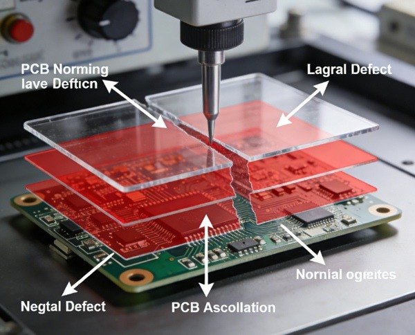
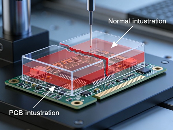
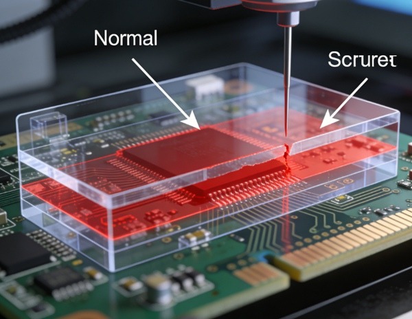
PCB-delaminatie is een van de meest destructieve en vaak onomkeerbare faalwijzen in printplaten.
In tegenstelling tot oppervlaktedefecten treedt delaminatie op binnen de PCB-structuurkoperen lagen of diëlektrische materialen te scheiden en de mechanische sterkte, elektrische isolatie en betrouwbaarheid op lange termijn in gevaar te brengen.
Dit artikel legt het uit:
- Wat PCB delaminatie is
- Waarom het gebeurt
- Hoe fabrikanten het detecteren en voorkomen
Inhoudsopgave
Wat is PCB-vervuiling?
PCB delaminatie verwijst naar de verlies van hechting tussen lagen binnen een printplaat.
Het kan voorkomen tussen:
- Koperfolie en diëlektricum
- Aangrenzende diëlektrische lagen
- Interfaces van hars en glasvezel
Als delaminatie eenmaal begint, plant het zich vaak voort onder thermische of mechanische spanning.
Veelvoorkomende symptomen van PCB-vervuiling
Delaminatie is in het begin niet altijd zichtbaar.
Typische symptomen
- Blaarvorming of borrelen na het solderen
- Interne holtes gedetecteerd met röntgenstralen
- Plotselinge daling van de isolatieweerstand
- Mechanische zwakte tijdens assemblage
Detectiemethoden:
Röntgeninspectie bij PCB-productie
Primaire oorzaken van PCB-vervuiling
H3: Overmatige vochtabsorptie
Vocht in PCB-materialen zet snel uit tijdens het solderen of reflowen.
Deze uitzetting creëert interne druk die lagen kan scheiden.
Bijdragende factoren zijn onder andere:
- Onjuiste materiaalopslag
- Omgevingen met een hoge luchtvochtigheid
- Lange belichting voor montage
Verkeerde lamineerparameters
Lamineren is een kritisch proces bij de vervaardiging van meerlagige PCB's.
Delaminatie kan het gevolg zijn van:
- Onvoldoende lamineringsdruk
- Onvoldoende harsstroom
- Verkeerde uithardingstemperatuur of -tijd
Procesoverzicht:
PCB lamineerproces uitgelegd
Materiaal Onverenigbaarheid
Niet alle PCB-materialen hechten even goed.
Risicofactoren zijn onder andere:
- Mengen van materialen met verschillende glasovergangstemperaturen (Tg)
- Koperfolie met lage afpelsterkte
- Slechte hars-glas hechting
De materiaalselectie heeft een grote invloed op het risico op delaminatie.
Thermische stress en herhaalde verhitting
Herhaalde thermische cycli veroorzaken:
- Z-as expansiespanning
- Vermoeiing bij koper-hars interfaces
Printplaten met veel lagen zijn bijzonder kwetsbaar.
Betrouwbaarheidslink:
PCB thermische betrouwbaarheidstesten
Ontwerpfactoren die het risico op delaminatie verhogen
Ontwerpbeslissingen vergroten vaak het risico op delaminatie.
Ontwerppraktijken met een hoog risico
- Zeer dunne diëlektrische lagen
- Onbalans in hoge koperdichtheid
- Grote koperen vlakken zonder reliëf
- Onvoldoende tussenruimte bij de randen van de printplaat
Vroegtijdige DFM-beoordeling helpt deze risico's te beperken.
Hoe PCB-vervuiling wordt gedetecteerd
Algemene detectiemethoden
- Röntgeninspectie
- Doorsnede-analyse
- Thermische belastingstesten
- Visuele inspectie na het solderen
Inspectiehub:
PCB-inspectie en -testen uitgelegd
PCB-vervuiling voorkomen
Gecontroleerde materiaalopslag
- Vacuümverpakking
- Temperatuur- en vochtigheidsbewaking
- Juiste uitbakprocedures
Geoptimaliseerde lamineercontrole
- Geverifieerde drukprofielen
- Gecontroleerde harsstroom
- Consistente uithardingscycli
Praktijken voor ontwerp op betrouwbaarheid
- Uitgebalanceerde koperdistributie
- Voldoende diëlektrische dikte
- Verificatie van materiaalcompatibiliteit
Relatie tussen delaminatie en andere PCB-defecten
Delaminatie veroorzaakt vaak secundaire defecten:
- Via kraken
- CAF-vorming
- Isolatiebreuk
Verwante mislukkingen:
Veelvoorkomende PCB-fouten uitgelegd
Industrieel perspectief op Delaminatiecontrole
In de moderne PCB-productie wordt delaminatie voorkomen door:
- Materiaalkwalificatie
- Procesvensterbesturing
- Inspectie feedback loops
Fabrikanten zoals TOPFAST behandelen delaminatie als een Betrouwbaarheidsprobleem op systeemniveauen niet slechts een enkel procesdefect.
Conclusie
PCB delaminatie is een complexe foutmodus die beïnvloed wordt door materialen, ontwerp en productieomstandigheden.
Hoewel het niet altijd kan worden geëlimineerd, kan het wel effectief gecontroleerd door:
- Juiste materiaalbehandeling
- Geoptimaliseerde lamineerprocessen
- Doordachte ontwerpbeslissingen
Het begrijpen van delaminatiemechanismen is essentieel voor het bouwen van betrouwbare PCB's die lang meegaan.
PCB-vervuiling FAQ
A: Nee. Als er eenmaal delaminatie optreedt, is de printplaat meestal onbruikbaar.
A: Het vermindert het risico, maar neemt het niet weg.
A: Ja, vooral bij thermische cycli of hoge vochtigheid.
A: Ja, door de hogere interne spanning.
A: Vaak pas na stress of geavanceerde inspectie.