Etsen is het proces dat verandert verguld koper in nauwkeurige circuitpatronen.
Hoewel het er op het eerste gezicht eenvoudig uitziet, is etsen een van de moeilijkste dingen die je kunt doen. meest opbrengstgevoelige stappen in PCB-productie.
Vanuit het oogpunt van de fabrikant leidt een slechte controle op het etsen tot:
- Variatie in lijndikte
- Korte broeken en openingen
- Laag rendement
- Hogere productiekosten
Dit artikel legt uit hoe het etsen van PCB's werkt, wat de kwaliteit van het etsen beïnvloedt en hoe fabrikanten zoals TOPFAST opbrengstcontrole om een consistente, kosteneffectieve PCB-productie te garanderen.
Inhoudsopgave
Wat is PCB-etsen?
PCB-etsen is een chemisch proces dat verwijdert ongewenst koper van de printplaat, zodat alleen het ontworpen circuitpatroon overblijft.
Ets wordt toegepast op:
- Binnenlagen
- Buitenlagen
Het doel is om nauwkeurige spoorbreedte, -afstand en -geometrie volgens ontwerpspecificaties.
Soorten PCB-etsprocessen
Etsen van de binnenste laag
De binnenlaag wordt geëtst:
- Voor laminering
- Op dunne koperfolie
Het is zeer gevoelig omdat:
- Defecten kunnen niet worden gerepareerd na lamineren
- De opbrengst van de binnenlaag beïnvloedt de hele PCB-stapel
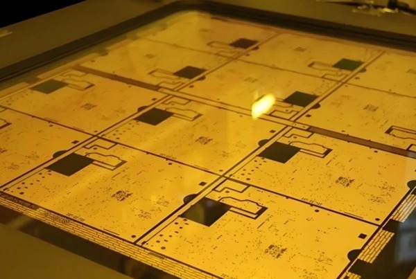
Buitenste laag etsen
De buitenste laag wordt geëtst:
- Na koperplateren
- Op dikkere koperlagen
Het etsen van de buitenste laag moet rekening houden met:
- Dikte geplateerd koper
- Uniformiteit over het paneel
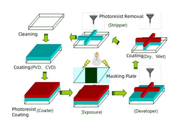
Stap voor stap PCB-etsproces
Stap 1 - Voorbereiding harspatroon
Een resist laag beschermt de koperen gebieden die na het etsen over moeten blijven.
De nauwkeurigheid van het patroon in dit stadium bepaalt de uiteindelijke geometrie van het spoor.
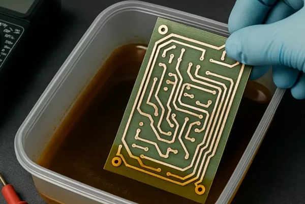
Stap 2 - Chemisch etsen
Chemische oplossingen verwijderen selectief blootgesteld koper.
Belangrijkste procesvariabelen:
- Concentratie van het etsmiddel
- Temperatuur
- Spuitdruk
- Etstijd
Het beheersen van deze variabelen is essentieel voor stabiele resultaten.
Stap 3 - Verzet strippen
Na het etsen wordt de resterende weerstand verwijderd, waardoor de afgewerkte kopersporen zichtbaar worden.
Veelvoorkomende etstefecten en hun invloed
Over-Etching
Oorzaken:
- Overmatige etstijd
- Agressieve chemie
Resultaten:
- Verminderde spoorbreedte
- Verhoogde impedantie
- Potentieel opent
Onderets
Oorzaken:
- Onvoldoende etstijd
- Zwakke etsactiviteit
Resultaten:
- Overblijvend koper
- Kortsluiting tussen sporen
Onderbieding
Etchant verwijdert koper zijwaarts onder de resist, waardoor de spoorbreedte afneemt.
Onderbieding wordt ernstiger met:
- Dikker koper
- Fijnere spoorontwerpen
Wat is opbrengst bij printplaatproductie?
Opbrengst verwijst naar de percentage borden dat voldoet aan de specificaties na productie.
Hoog rendement betekent:
- Lagere kosten per eenheid
- Stabiele kwaliteit
- Voorspelbare levering
Lage opbrengst leidt tot:
- Schroot
- Verwerken
- Hogere totale kosten
Hoe etsen het productierendement beïnvloedt
Etsen heeft een directe invloed op de opbrengst omdat:
- Spoordefecten veroorzaken elektrische storing
- Binnenlaagdefecten vermenigvuldigen zich bij panelen
- Kleine variaties beïnvloeden ontwerpen met hoge dichtheid
Vanuit het oogpunt van de fabrikant is etsen een van de hoogste aangrijpingspunten voor opbrengstverbetering.
Ontwerpfactoren die het etsrendement beïnvloeden
Opbrengst verbetert bij ontwerpen:
- Vermijd onnodig fijne sporen
- Consistente lijndikte behouden
- Koperverdeling in evenwicht
- Gebruik de door de fabrikant aanbevolen minimumafstanden
DFM beoordeling brengt vaak vroegtijdig ets-gerelateerde risico's aan het licht.
Hoe fabrikanten de opbrengst van etsen controleren
Procesbewaking
De belangrijkste besturingselementen zijn:
- Continue chemieanalyse
- Kalibratie van apparatuur
- Real-time lijndiktemeting
Paneelniveau optimalisatie
Fabrikanten optimaliseren:
- Paneelindeling
- Koperbalans
- Gelijkmatig etsen op het paneel
Inspectie en feedback
AOI en elektrische testen feedback geven aan:
- etsparameters aanpassen
- Processtabiliteit verbeteren
Bij TOPFAST worden opbrengstgegevens actief gebruikt om etsprocessen te verfijnen en herhaling te voorkomen.
Kostenimpact van etsen en opbrengstverlies
Lage opbrengst verhoogt kosten door:
- Afgedankte materialen
- Extra arbeid
- Vertragingen in de productie
Het verbeteren van het etsrendement is vaak effectiever dan kosten snijmateriaal bij het verlagen van de printplaatprijs.
Perspectief van de fabrikant: TOPFAST's opbrengstgerichte strategie voor etsen
TOPFAST controleert het etsrendement door:
- Gestandaardiseerde procesvensters
- Conservatieve ontwerpaanbevelingen
- Vroege DFM-feedback
- Continue opbrengstbewaking
De focus ligt op constante kwaliteit en schaalbare productieen niet alleen voldoen aan minimale toleranties.
Conclusie
PCB-etsen is een bedrieglijk eenvoudig proces met een grote invloed op opbrengst, kosten en betrouwbaarheid.
Door te begrijpen hoe etsen werkt en wat de opbrengst beïnvloedt, kunnen ontwerpers en kopers slimmere beslissingen nemen:
- Productierisico verminderen
- Lagere totale kosten
- Productbetrouwbaarheid verbeteren
Met een opbrengstgerichte productiebenadering, TOPFAST zorgt voor een stabiele etskwaliteit die betrouwbare PCB-productie op schaal ondersteunt.
Gerelateerde lezen
PCB Fabricageproces PCB Fabricageproces
Veelgestelde vragen over het rendement van etsen
A: PCB-etsen is een chemisch proces dat ongewenst koper verwijdert om circuitpatronen te vormen.
A: Over-etsen wordt veroorzaakt door een te lange etstijd of te agressieve chemische oplossingen.
A: Slechte controle op het etsen leidt tot spoordefecten, waardoor de opbrengst daalt en de kosten stijgen.
A: Ja. Ontwerpen met een redelijke spoorbreedte en -afstand verbeteren het etsrendement aanzienlijk.
A: TOPFAST gebruikt gestandaardiseerde processen, real-time controle en DFM-feedback om een stabiele etsopbrengst te behouden.