Gedrukte schakelingen (PCB's) vormen de basis van moderne elektronische producten. Hoewel veel ingenieurs zich richten op PCB-ontwerp, zijn er minder die volledig begrijpen hoe een PCB eigenlijk wordt gemaakt.
Het PCB productieproces begrijpen helpt:
- Ontwerp verbeteren met het oog op maakbaarheid (DFM)
- Productiekosten verlagen
- Vermijd kwaliteitsproblemen
- Effectiever communiceren met PCB-fabrikanten
Dit artikel biedt een duidelijke, stapsgewijze uitleg van het PCB fabricageprocesgebaseerd op echte productiepraktijken gebruikt door TOPFAST, een professionele PCB-fabrikant die prototype- en massaproductie ondersteunt.
Inhoudsopgave
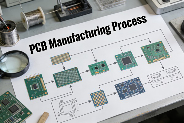
Overzicht van het productieproces van PCB's
Hoewel de complexiteit van PCB's kan variëren, volgen de meeste starre PCB's dezelfde productiestroom:
- Fabricage binnenlaag
- Lagen uitlijnen en lamineren
- Boren
- Koperen beplating
- Beeldvorming en etsen van de buitenlaag
- Soldeermasker aanbrengen
- Afwerking oppervlak
- Zeefdruk
- Elektrisch testen en eindinspectie
Elke stap heeft direct invloed op kwaliteit, opbrengst en kosten.
Stap 1 - Binnenlaag Fabricage
Beeldvorming binnenste laag
De productie begint met met koper beklede laminaatplaten. Het gewenste circuitpatroon wordt overgebracht op het koperoppervlak met behulp van een fotolak en UV-belichting.
Sleutelfactoren:
- Nauwkeurigheid spoorbreedte en -afstand
- Precisie foto-uitlijning
- Cleanroom-omgeving
Etsen van de binnenste laag
Ongewenst koper wordt chemisch weg geëtst, waardoor de vereiste circuitsporen overblijven.
Vanuit een productieperspectief:
- Fijnere sporen maken etsen moeilijker
- Over-etsen of onder-etsen beïnvloedt de opbrengst
Bij TOPFAST worden de parameters voor het etsen van de binnenlaag geoptimaliseerd om een balans te vinden tussen precisie en productiestabiliteit.
Stap 2 - Lagen uitlijnen en lamineren
Voor meerlagige PCB's worden binnenlagen gestapeld met prepreg en buitenste koperfolies.
Lamineerproces
- Hitte en druk verbinden alle lagen
- Nauwkeurige uitlijning zorgt voor nauwkeurige viaverbindingen
Impact op kosten en kwaliteit:
- Meer lagen verhogen lamineercycli
- Sequentieel lamineren verhoogt complexiteit en kosten
Stap 3 - Boren
Boren creëert gaten voor vias en afleidingen van componenten.
Mechanisch boren
Gebruikt voor:
- Gaten
- Grotere gaten
De boorkosten nemen toe met:
- Kleinere gatdiameters
- Hogere beeldverhoudingen
- Hoge boortellingen
Laserboren (geavanceerde printplaten)
Laserboren wordt gebruikt voor:
- Microvia's in HDI PCB's
Dit proces vereist gespecialiseerde apparatuur en verhoogt de productiekosten.
Stap 4 - Verkoperen
Na het boren moeten de gaten elektrisch geleidend zijn.
Afzetting van elektrolytisch koper
Een dunne koperlaag wordt afgezet binnen de geboorde gaten om een elektrische verbinding tussen de lagen mogelijk te maken.
Galvanisch verzinken
Extra koper is verguld:
- Vias versterken
- De vereiste koperdikte bereiken
De uniformiteit van het plateren heeft een directe invloed op de betrouwbaarheid, vooral voor toepassingen met hoge stromen of hoge betrouwbaarheid.
Stap 5 - Afbeelden en etsen van de buitenste laag
Het circuitpatroon van de buitenste laag wordt gevormd met een proces dat vergelijkbaar is met dat van de binnenste lagen.
Belangrijkste uitdagingen:
- Nauwkeurigheid behouden na uitplaten
- Koperdikte regelen
- Kortsluiting of openingen voorkomen
De verwerking van de buitenlaag heeft een grote invloed op uiteindelijke opbrengst.
Stap 6 - Soldeermasker aanbrengen
Doel van soldeermasker
Soldeermasker:
- Beschermt kopersporen
- Voorkomt soldeerbruggen
- Verbetert de elektrische isolatie
Veel voorkomende kleuren zijn groen, zwart, blauw en rood. Groen blijft de meest kosteneffectieve en meest gebruikte optie.
Kwaliteitsfactoren soldeermasker
- Nauwkeurigheid registratie
- Dikte masker
- Openingsdefinitie
Een slechte kwaliteit van het soldeermasker kan later assemblagefouten veroorzaken.
Stap 7 - Afwerking oppervlak
De oppervlakteafwerking beschermt blootliggende koperen pads en garandeert soldeerbaarheid.
Algemene opties voor oppervlakteafwerking
- HASL: Kosteneffectief, veel gebruikt
- ENIG: Vlak oppervlak, hogere betrouwbaarheid
- OSP: Lage kosten, beperkte houdbaarheid
TOPFAST adviseert oppervlakteafwerkingen op basis van toepassingsvereisten in plaats van standaardvoorkeuren.
Stap 8 - Zeefdruk
Zeefdruk voegt toe:
- Referentieaanduidingen voor onderdelen
- Polariteitsmarkeringen
- Logo's of herkenningstekens
Hoewel ze niet elektrisch werken, verbetert een heldere zeefdruk de nauwkeurigheid van de montage en het onderhoud.
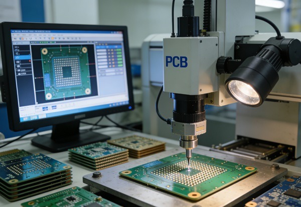
Stap 9 - Elektrische testen en eindinspectie
Elektrische testen
Elektrische tests verifiëren dit:
- Continuïteit
- Isolatie
- Afwezigheid van korte broeken en open
Deze stap is essentieel om functionele betrouwbaarheid te garanderen.
Eindinspectie
De eindinspectie kan het volgende omvatten:
- Visuele inspectie
- AOI (geautomatiseerde optische inspectie)
- Dimensionale controlesant ~4.3-4.8)
Bij TOPFAST zijn de inspectienormen afgestemd op IPC-vereisten en klantspecificaties.
Hoe het PCB productieproces de kosten en kwaliteit beïnvloedt
Elke productiestap introduceert:
- Procesvariabiliteit
- Rendementsoverwegingen
- Gevolgen voor de kosten
Veelvoorkomende kostenveroorzakers zijn onder andere:
- Hoog aantal lagen
- Kleine boormaten
- Nauwe toleranties
- Geavanceerde oppervlakteafwerkingen
Inzicht in het volledige proces stelt ontwerpers in staat om PCB-ontwerpen optimaliseren voor zowel kosten als produceerbaarheid.
Het perspectief van de fabrikant: Hoe TOPFAST de printplaatproductie optimaliseert
Als PCB-fabrikant richt TOPFAST zich op:
- Standaardisatie van processen
- Vroege DFM-feedback
- Opbrengstgestuurde besluitvorming
- Stabiele en schaalbare productie
In plaats van onnodige geavanceerde processen te pushen, legt TOPFAST de nadruk op productievriendelijke ontwerpen die een consistente kwaliteit leveren.
Conclusie
Het PCB productieproces is een zorgvuldig gecontroleerde opeenvolging van stappen die elk bijdragen aan de prestaties, betrouwbaarheid en kosten van de uiteindelijke printplaat.
Door te begrijpen hoe PCB's worden gemaakt - van de fabricage van de binnenste laag tot en met de eindinspectie - kunnen ontwerpers en inkopers betere ontwerp- en inkoopbeslissingen nemen.
Met een productiegerichte aanpak, TOPFAST helpt klanten om complexe ontwerpen om te zetten in betrouwbare, kosteneffectieve PCB's.
PCB stap voor stap productieproces FAQ
A: Standaard PCB productie duurt meestal 5-10 werkdagen, afhankelijk van de complexiteit en de hoeveelheid.
A: Elke stap is belangrijk, maar boren en plateren zijn cruciaal voor de elektrische betrouwbaarheid.
A: Ja. Voor meerlaagse printplaten zijn extra lamineer- en uitlijnstappen nodig.
A: Ja. Ontwerpen die zijn afgestemd op de productiemogelijkheden verbeteren de opbrengst en verlagen de kosten.
A: TOPFAST maakt gebruik van gestandaardiseerde processen, DFM-beoordeling en uitgebreide inspectie om een consistente kwaliteit te garanderen.