PCB-productie is een meerstaps, streng gecontroleerd proces waar kleine afwijkingen kunnen leiden tot betrouwbaarheidsproblemen, opbrengstverlies of hogere kosten.
Hoewel veel bronnen PCB-fabricage op een hoog niveau beschrijven, is het begrijpen van hoe elke productiestap interageert met de volgende is essentieel voor:
- Ontwerp van produceerbare printplaten
- Kosten beheersen
- Betrouwbaarheid op lange termijn garanderen
Dit artikel biedt een stapsgewijs overzicht van het PCB fabricageprocesmet links naar diepgaande uitleg over elke kritieke fase.
Het perspectief weerspiegelt echte productiepraktijken die worden gebruikt door professionele printplaatfabrikanten zoals TOPFASTwaar processtabiliteit en opbrengstbeheersing kernprioriteiten zijn.
Inhoudsopgave
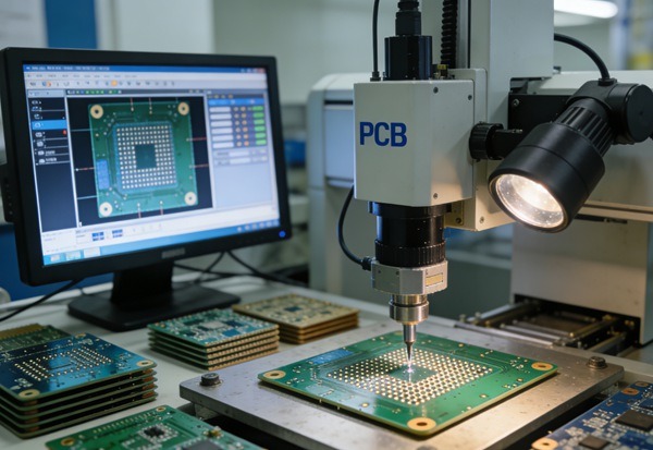
Overzicht van de PCB productieproces ~4.3-4.8)
Een typische workflow voor PCB-productie omvat:
- Fabricage binnenlaag
- Boren (mechanisch of laser)
- Koperen beplating
- Patroon etsen
- Inspectie en opbrengstcontrole
Elke stap bouwt voort op de vorige. Fouten vroeg in het proces kunnen later vaak niet meer gecorrigeerd worden.
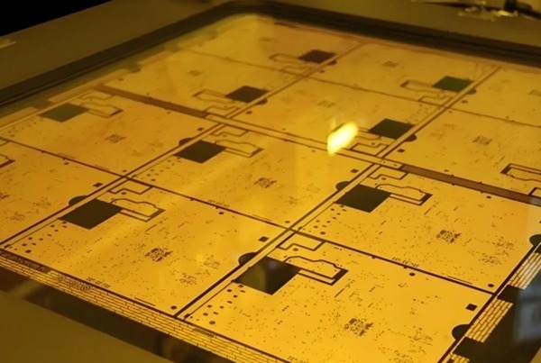
Binnenlaag Fabricage
De fabricage van de binnenlaag is de basis van meerlagige PCB-productie.
In dit stadium:
- Koperfolie wordt gedessineerd om interne circuits te vormen
- Maatnauwkeurigheid is cruciaal
- Defecten worden na het lamineren permanent in de stapel opgesloten
Omdat binnenlagen na het lamineren niet meer gerepareerd kunnen worden, passen fabrikanten strenge procescontroles en inspectienormen toe.
Zie voor een gedetailleerde uitleg over het prepareren van de binnenlaag, beeldvorming en etsen:
Uitleg over de fabricage van de binnenste laag
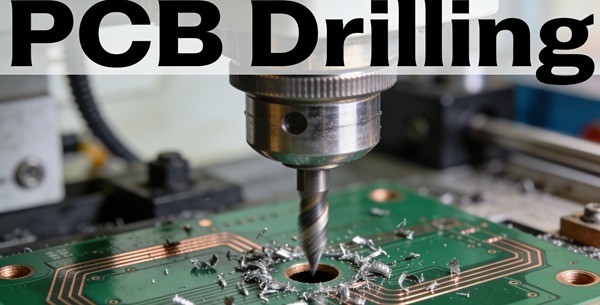
PCB boren: Tussenlaagverbindingen maken
Boren creëert de gaten die later vias en through-hole verbindingen zullen worden.
Er worden twee primaire boormethoden gebruikt:
- Mechanisch boren
- Laserboren
Elke methode heeft nadelen:
- Gatgrootte
- Beeldverhouding
- Kosten
- Betrouwbaarheid
Onjuist boren heeft een directe invloed op de kwaliteit van het plateren en op de betrouwbaarheid.
Lees om te begrijpen wanneer mechanisch boren of laserboren geschikt is:
PCB-boren vs. Laserboren
Koperplateerproces
Verkoperen verandert geboorde gaten in elektrisch geleidende verticale verbindingen.
Het platingproces omvat:
- Afzetting van elektrolytisch koper
- Dikteopbouw van elektrolytisch koper
De kwaliteit van het plateren is bepalend:
- Via muursterkte
- Thermische cyclische prestaties
- Stroomvoerend vermogen
Inconsistent plateren is een veel voorkomende oorzaak van defecten in de praktijk, zelfs wanneer printplaten de eerste elektrische tests doorstaan.
Zie voor een volledig overzicht van beplatingsstappen en betrouwbaarheidsoverwegingen:
Verkoperen bij PCB Fabricage Uitgelegd
PCB-etsen en circuitvorming
Ets verwijdert ongewenst koper om het uiteindelijke circuitpatroon te definiëren.
Deze stap moet in evenwicht zijn:
- Koperdikte
- Nauwkeurigheid lijndikte
- Afstandscontroleant ~4.3-4.8)
Over-etsen of onder-etsen leidt tot:
- Opens of shorts
- Impedantievariatie
- Lagere productieopbrengst
De prestaties van het etsen worden steeds kritischer naarmate ontwerpen steeds fijnere sporen en meer lagen bevatten.
Lees voor een diepgaande blik op de chemie van het etsen en de invloed op het rendement:
PCB-etsproces en opbrengstcontrole uitgelegd
Opbrengstcontrole in het hele productieproces
Opbrengst wordt niet in één stap gecontroleerd - het is de resultaat van cumulatieve processtabiliteit.
De belangrijkste rendementsfactoren zijn:
- Nauwkeurigheid binnenlaag
- Boorkwaliteit
- Uniformiteit van het plateren
- Etsconsistentie
Professionele printplaatfabrikanten controleren continu de opbrengstgegevens om:
- Procesdrift identificeren
- Ontwerpregels optimaliseren
- Minder uitval en herbewerking
Bij TOPFAST wordt opbrengstfeedback geïntegreerd in DFM-beoordelingen om klanten te helpen verborgen productierisico's te vermijden voordat de productie begint.
Zie voor een productiegericht overzicht van rendementsbepalende factoren:
PCB-etsproces en opbrengstcontrole uitgelegd
Hoe ontwerpbeslissingen het productieproces beïnvloeden
Vanuit het oogpunt van productie zijn veel problemen met PCB's te wijten aan ontwerpkeuzes zoals:
- Te fijne spoorbreedten
- Vias met hoge hoogte-breedteverhouding
- Ongebalanceerde koperdistributie
- Te krappe toleranties
Vroegtijdige samenwerking tussen ontwerpers en fabrikanten helpt om de ontwerpintentie af te stemmen op de procesmogelijkheden.
Deze aanpak vermindert:
- Iteraties
- Vertragingen in de productie
- Totale eigendomskosten
Perspectief van de fabrikant: Procesintegratie bij TOPFAST
Als professionele PCB-fabrikant benadert TOPFAST PCB-fabricage als een geïntegreerd systeemgeen geïsoleerde stappen.
De belangrijkste principes zijn:
- Stabiele procesvensters
- Vroegtijdige identificatie van DFM-risico's
- Opbrengstgestuurde optimalisatie
- IPC-kwaliteitsnormen
In plaats van alleen te focussen op minimumspecificaties, ligt de nadruk op herhaalbaarheid, betrouwbaarheid en schaalbare productie.
Conclusie
Het PCB-productieproces is een opeenvolging van onderling afhankelijke stappen waarbij de kwaliteit geleidelijk wordt opgebouwd en niet aan het einde wordt geïnspecteerd.
Door te begrijpen hoe binnenlaagvervaardiging, boren, verkoperen en etsen samenwerken, kunnen ingenieurs en inkopers:
- Betere ontwerpbeslissingen nemen
- Productierisico verminderen
- Beheers de kosten zonder aan kwaliteit in te boeten
Dit overzicht dient als toegangspoort tot diepere technische uitleg van elke kritieke fase en weerspiegelt praktijkvoorbeelden van ervaren printplaatfabrikanten zoals TOPFAST.