تدمج تقنية تجميع ثنائي الفينيل متعدد الكلور (SiP) رقائق متعددة في حزمة واحدة، مما يقلل من حجم وحدة الاستشعار بنسبة 70%. (PCBA) هي الخطوة التي يتم فيها يتحول ثنائي الفينيل متعدد الكلور العاري إلى لوحة إلكترونية وظيفيةيركز تصنيع ثنائي الفينيل متعدد الكلور على مرحلة تصنيع اللوحة العارية، والتي تشكل أساس سير عمل تصنيع ثنائي الفينيل متعدد الكلور الكامل. وتتضمن وضع المكونات، واللحام، والاختبارات الدقيقة
تؤثر جودة التجميع بشكل مباشر على:
- الوظائف الكهربائية
- موثوقية المنتج
- عائد التصنيع
في توب فاست، يتم التعامل مع التجميع على أنه عملية مدفوعة بالعائدوضمان أن تكون اللوحات فعالة وقوية.
لمعرفة خلفية عن علاقة تجميع ثنائي الفينيل متعدد الكلور بالتصنيع، انظر: تصنيع ثنائي الفينيل متعدد الكلور مقابل تجميع ثنائي الفينيل متعدد الكلور
جدول المحتويات
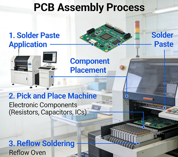
تقنية التركيب على السطح تجميع (SMT)
ما هو تجميع SMT؟
يتضمن تجميع SMT التركيب مكونات مثبتة على السطح مباشرة على وسادات ثنائي الفينيل متعدد الكلور باستخدام:
- معجون اللحام
- ماكينات الالتقاط والوضع
- إعادة تدفق اللحام
SMT هو سريعة ودقيقة ومناسبة للألواح عالية الكثافةيشيع استخدامها في الإلكترونيات الاستهلاكية والاتصالات وأجهزة إنترنت الأشياء.
تحديات SMT
- تتطلب المكونات رفيعة المستوى دقة فائقة في الموضع
- يمكن أن يؤدي الإجهاد الحراري أثناء إعادة التدفق إلى تلف مركبات ثنائي الفينيل متعدد الكلور إذا كانت الطبقات الداخلية أو طلاء النحاس غير متناسقة
- تزيد الألواح عالية الكثافة من حساسية المحصول
في TOPFAST، يتم تنسيق تجميع SMT بعناية مع بيانات التصنيع من أجل تقليل العيوب وتحسين الإنتاجية.
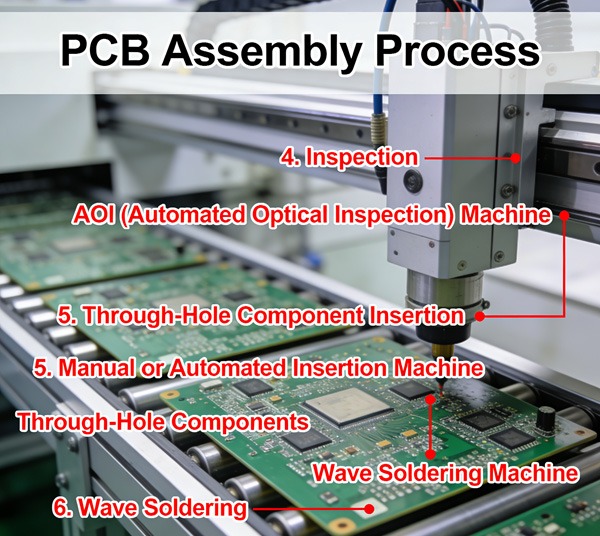
التجميع عبر فتحة التجميع
ما هو التجميع عبر الفتحة؟
يقوم التجميع عبر الفتحات بإدخال المكونات ذات الأسلاك في ثقوب مثقوبة وملحومة باستخدام:
- اللحام الموجي (اللحام الشامل)
- اللحام اليدوي (للنماذج الأولية أو الألواح منخفضة الحجم)
لا يزال يتم استخدام الثقب العابر على نطاق واسع في:
- القوة الميكانيكية
- مكونات عالية الطاقة
- الموصلات والحزم الكبيرة
سير عمل التجميع عبر الفتحات
- ملء الثقب/إدخال المكونات - أدخل أسلاك المكونات في الفتحات المطلية
- اللحام - لحام موجي أو لحام انتقائي لتأمين المكونات
- الفحص - فحوصات بصرية أو بالهيئة العربية للتصنيع لجودة اللحام
تتأثر جودة الحفر والطلاء بشكل مباشر بما يلي حفر ثنائي الفينيل متعدد الكلور مقابل الحفر بالليزرو شرح عملية الطلاء بالنحاس.
التحديات العابرة للثقوب
- تقلل الثقوب غير المصفوفة أو سيئة الطلاء من موثوقية وصلة اللحام
- يزيد التجميع اليدوي من تكلفة العمالة واحتمال حدوث خطأ بشري
- تتطلب مساحة أكبر على اللوحة أكثر من SMT
يجمع TOPFAST بين الحفر الدقيق والطلاء الدقيق مع تحسين التجميع لزيادة العائد من خلال الفتحة إلى أقصى حد.
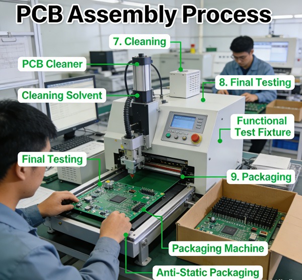
الاختبار ومراقبة الجودة في التجميع
الاختبار داخل الدائرة (ICT)
فحوصات تكنولوجيا المعلومات والاتصالات
- السراويل القصيرة
- يفتح
- قيم المكونات الصحيحة
الاختبار الوظيفي
يحاكي الاختبار الوظيفي التشغيل في العالم الحقيقي للتحقق من أن اللوحة تعمل كما تم تصميمها.
الاختبار هو نقطة التحقق النهائية لضمان مطابقة خطوات التصنيع والتجميع للمواصفات. انظر شرح عملية الحفر والتحكم في الإنتاجية لكيفية تأثير جودة المرحلة المبكرة على نتائج الاختبار.
اعتبارات العائد التجميعي
العائد
- جودة التصنيع (مثل الطبقات الداخلية والحفر والطلاء)
- دقة تحديد موضع المكونات
- معلمات اللحام
- تصميم اللوحة (الحرارة، التباعد، حجم اللوحة)
يقلل التجميع عالي الإنتاجية:
- إعادة العمل
- الخردة
- التكلفة الإجمالية للإنتاج
- ارجع إلى تصنيع ثنائي الفينيل متعدد الكلور مقابل تجميع ثنائي الفينيل متعدد الكلور لمعرفة كيف تشمل اعتبارات العائد كلتا العمليتين.
عوامل التكلفة في التجميع
محركات التكلفة الرئيسية:
- نوع المكون والتعبئة والتغليف
- كثافة اللوح وعدد الطبقات
- حجم التجميع (النموذج الأولي مقابل الإنتاج الضخم)
- متطلبات الاختبار والفحص
يتطلب تحسين التجميع الأمثل دون التضحية بالجودة ما يلي المواءمة الوثيقة بين عمليات التصميم والتصنيع والتجميع.
الخاتمة
يعمل تجميع ثنائي الفينيل متعدد الكلور على تحويل اللوحة العارية إلى منتج إلكتروني يعمل بكامل طاقته.
عمليات SMT والعمليات عبر الفتحاتإلى جانب الاختبارات القوية، تحدد موثوقية المنتج النهائي.
من الضروري تحقيق التكامل مع جودة التصنيع:
- عائد مرتفع
- إنتاج فعال من حيث التكلفة
- الموثوقية على المدى الطويل
الأسئلة الشائعة حول عملية تجميع ثنائي الفينيل متعدد الكلور
ج: يتضمن تجميع ثنائي الفينيل متعدد الكلور تركيب المكونات الإلكترونية على ثنائي الفينيل متعدد الكلور المصنّع باستخدام تقنيات SMT أو من خلال ثقب، ثم الفحص والاختبار.
ج: تقوم SMT بتركيب المكونات على سطح ثنائي الفينيل متعدد الكلور، بينما تقوم الثقب العابر بإدخال أسلاك المكونات في الثقوب المحفورة ولحامها.
ج: يمكن أن تتسبب الطبقات غير المتناسقة أو الثقوب المحفورة بشكل سيئ أو الطلاء غير المتناسق في حدوث عيوب لحام وتقلل من إنتاجية التجميع.
ج: يشيع استخدام الفحص البصري الآلي (AOI) والفحص بالأشعة السينية والاختبار داخل الدائرة والاختبار الوظيفي.
ج: تعمل TOPFAST على مواءمة عمليات التصنيع والتجميع، وتطبق عمليات الفحص الآلي واليدوي، وتستخدم التحسين القائم على الإنتاجية لتحقيق إنتاج موثوق به