Joustavien piirilevyjen lopullinen opas: tyypit, suunnittelu ja sovellukset
Sisällysluettelo
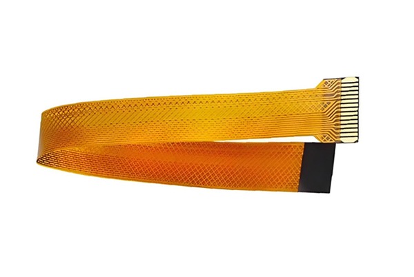
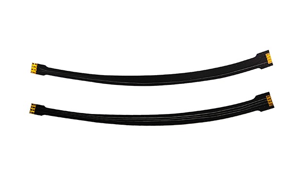
Mikä Joustavat PCB:t?
Joustavat painetut piirilevyt (FPC) käyttävät joustavia substraatteja, kuten polyimidiä, tukemaan taivutusta, taittoa tai vääntöä, minkä ansiosta niitä voidaan käyttää laajasti tiheään integrointiin ja dynaamisiin taivutustilanteisiin. Tärkeimmät ominaisuudet ovat:
- Kevyt ja ohut: 60 %:n paino- ja tilansäästö verrattuna jäykkään piirilevyyn.
- Dynaaminen taivutuskyky: Kestää jopa 500 miljoonaa toistettua taivutusta (360° täysi kulma).
- Ympäristön sopeutumiskyky: Kestää korkeita lämpötiloja (jopa 400 °C), tärinää ja kemiallista korroosiota.
Joustavien piirilevyjen tyyppien vertailu
| Tyyppi | Rakenteelliset ominaisuudet | Sovellukset | Valmistuksen monimutkaisuus |
|---|---|---|---|
| Yksipuolinen joustava PCB | Yksikerroksinen polyimidi + kuparifolio + päällyskerros | Yksinkertaiset liittimet, anturit | ★☆☆☆☆ |
| Kaksipuolinen joustava PCB | Kaksipuoliset kuparikerrokset + pinnoitetut läpivientiliitännät | Autoteollisuuden kojelaudat, teollisuuden ohjauslaitteet | ★★★☆☆ |
| Monikerroksinen joustava PCB | ≥3 kuparikerrosta + monimutkaiset liitännät | Lääketieteelliset laitteet, ilmailu- ja avaruusteollisuuden instrumentit | ★★★★★ |
Tärkeimmät tekniset parametrit
1. Taivutussäteen laskeminen
Kaava: Pienin taivutussäde = (levyn paksuus × joustavuuskerroin) / 2
- Tyypillinen arvo: 0,4 mm paksu levy voi taipua 90° kulmaan.
- Turvallisuusohje: Suositeltu taivutussäde ≤1 mm; 180°:n taivutukset edellyttävät erityistä suunnittelua.
2. Materiaalin koostumus
- Substraatti: Pääasiassa polyimidi (PI), erinomainen korkean lämpötilan kestävyys.
- ConductoressSuunnitteluohjeet:: Valssattu hehkutettu kupari (dynaaminen taivutus) vs. sähköpinnoitettu kupari (staattiset sovellukset).
- Liimamateriaalit: Akryyli-/epoksihartsijärjestelmän laminaatit.
Jäykistimen suunnitteluohjeet
Toiminnallinen sijoitus:
┌──────────────────────────────┐
│ Mekaaninen tuki │ Estää liittimen alueen muodonmuutoksia │
├──────────────────────────────┤
│ Stressin hajautus │ Vähentää mekaanista rasitusta juotosliitoksissa │
├──────────────────────────────┤
│ Asennusasento │ Tarjoaa tukevan asennusrajapinnan │
└──────────────────────────────┘
Yleiset materiaalit: FR4 (0,2–0,5 mm), ruostumaton teräs (korkeataajuussovellukset).
Suunnitteluohjeet (rakenteinen tarkistuslista)
Jäljen asettelu
- Vältä suorakulmaisia jälkiä (käytä kaarevia siirtymiä).
- Porrasta jäljityskohdat ylä- ja alakerroksissa kaksipuolisissa levyissä.
- Lisää pisaranmuotoiset tyynyt kriittisiin kohtiin vahvistukseksi.
Taivutusalueen käsittely
- Käytä hatching-täyttöjä kiinteiden kuparitäyttöjen sijaan.
- Kielletään läpiviennit/tyynyt taivutusalueilla.
- päällysteen aukon tulisi olla 10 % suurempi kuin johtokerros.
Valmistukseen liittyvät seikat
- Paneelin asennuksessa on varattava 5 mm:n reuna.
- Määritä ZIF-liittimien paksuustoleranssiksi ±0,1 mm.
- Lisää optiset kohdistusmerkit.
Edut ja rajoitukset -analyysi
Edut:
- ✅ Kolmiulotteinen reititysominaisuus (säästää 40 % tilaa).
- ✅ Kestävyys mekaanista väsymistä vastaan (3 kertaa pidempi käyttöikä tärinäolosuhteissa).
- ✅ Korkea lämpötilavakaus (Tg-arvo >200 °C).
Sovelluksen rajoitukset:
- ⚠️ Kustannukset ovat 30–50 % korkeammat kuin jäykkien piirilevyjen.
- ⚠️ Vaikea korjata (vaatii erikoislaitteita).
- ⚠️ Herkkä naarmuille (vaatii rikkivapaata pakkausta).
Teollisuuden sovellusten jakelu
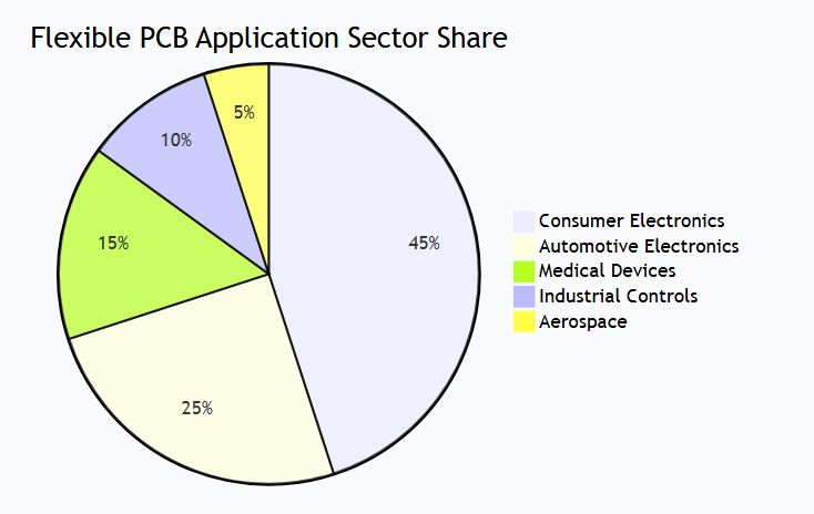
Tyypillisiä tilanteita:
- Älykellot: 360° taivutettavat näyttöliitännät.
- ADAS-järjestelmät: Tärinänkestävät anturipiirit.
- Endoskoopit: Tiheä biologisten signaalien siirto.
Erityiset valmistusprosessia koskevat huomautukset
- Kuparifolion valinta:
- Dynaamiset sovellukset: Valssattu hehkutettu (RA) kupari parempaa sitkeyttä varten.
- Staattiset sovellukset: Sähkökemiallisesti pinnoitettu (ED) kupari alhaisempien kustannusten saavuttamiseksi.
- Pinnan viimeistely:
- ENIG: Paras juotosliitoksen luotettavuus.
- OSP: Sopii lyhyille varastointijaksoille.
- Kova kullatus: Erityisesti ZIF-liittimille.
- Laadunvalvonta:
- Taivutustestaus: Vahvistettu IPC-6013-standardin mukaisesti.
- Lämpörasitustestaus: Juotoskestävyys 288 °C:ssa.
- Impedanssin säätö: ±10 % toleranssivaatimus.
Miksi ne eivät sovi kaikkiin tilanteisiin?
Merkittävistä eduista huolimatta jäykkiä ratkaisuja suositellaan seuraaviin kohteisiin:
Ammattilaisen neuvo: DFM-keskustelujen (Design for Manufacturability, valmistettavuuden suunnittelu) käymällä valmistajien kanssa konseptisuunnitteluvaiheessa voidaan vähentää kehitysriskejä yli 30 % ja optimoida valmistuskustannuksia. Joustavien piirilevyjen onnistunut käyttö riippuu materiaalien valinnan, mekaanisen suunnittelun ja valmistusprosessien tarkasta koordinoinnista.


Aiheeseen liittyvät viestit