La délamination des circuits imprimés est l'un des modes de défaillance les plus destructeurs et souvent irréversibles des circuits imprimés.
Contrairement aux défauts de surface, la délamination se produit à l'intérieur de la structure du PCBLa plupart du temps, la couche de cuivre ou les matériaux diélectriques sont séparés, ce qui compromet la résistance mécanique, l'isolation électrique et la fiabilité à long terme.
Cet article explique :
- Qu'est-ce que la délamination des PCB ?
- Pourquoi cela se produit-il ?
- Comment les fabricants les détectent et les préviennent
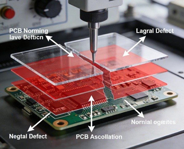
Table des matières
Qu'est-ce que le décollement des PCB ?
La délamination des PCB fait référence à la perte d'adhérence entre les couches à l'intérieur d'un PCB.
Elle peut survenir entre :
- Feuille de cuivre et diélectrique
- Couches diélectriques adjacentes
- Interfaces résine et fibre de verre
Une fois que la délamination commence, elle se propage souvent sous l'effet d'une contrainte thermique ou mécanique.
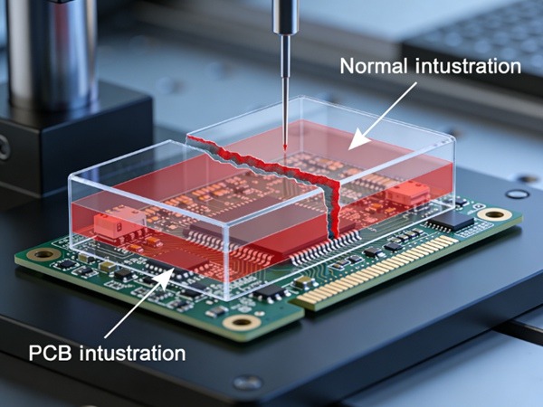
Symptômes courants de décollement des PCB
Le décollement n'est pas toujours visible au départ.
Symptômes typiques
- Formation de cloques ou de bulles après le brasage
- Vides internes détectés par rayons X
- Chute soudaine de la résistance d'isolement
- Faiblesse mécanique lors de l'assemblage
Méthodes de détection :
Inspection par rayons X dans la fabrication des circuits imprimés
Principales causes de décollement des PCB
H3 : Absorption excessive d'humidité
L'humidité piégée dans les matériaux des circuits imprimés se dilate rapidement pendant la soudure ou la refusion.
Cette expansion crée une pression interne qui peut séparer les couches.
Les facteurs qui y contribuent sont les suivants :
- Stockage inadéquat des matériaux
- Environnements à forte humidité
- Longue exposition avant l'assemblage
Paramètres de laminage incorrects
Le laminage est un processus critique dans la fabrication de circuits imprimés multicouches.
Le décollement peut résulter de :
- Pression de laminage insuffisante
- Débit de résine insuffisant
- Température ou durée de durcissement incorrecte
Aperçu du processus :
Explication du processus de lamination des circuits imprimés
Incompatibilité des matériaux
Tous les matériaux des circuits imprimés n'ont pas la même qualité d'adhérence.
Les facteurs de risque sont les suivants
- Mélange de matériaux ayant des températures de transition vitreuse (Tg) différentes
- Feuilles de cuivre à faible résistance au pelage
- Mauvaise adhérence de la résine au verre
Le choix des matériaux influence fortement le risque de délamination.
Stress thermique et chauffage répété
Les cycles thermiques répétés en sont la cause :
- Contrainte de dilatation selon l'axe Z
- Fatigue aux interfaces cuivre-résine
Les cartes à nombre élevé de couches sont particulièrement vulnérables.
Lien de fiabilité :
Test de fiabilité thermique des circuits imprimés
Facteurs de conception qui augmentent le risque de délamination
Les décisions de conception amplifient souvent le risque de délamination.
Pratiques de conception à haut risque
- Couches diélectriques très fines
- Déséquilibre de la densité de cuivre
- Grands plans de cuivre sans relief
- Espacement inadéquat près des bords du panneau
Un examen précoce de la DFM permet d'atténuer ces risques.
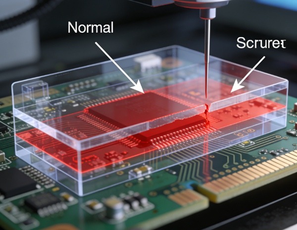
Comment le décollement des PCB est-il détecté ?
Méthodes de détection courantes
- Inspection par rayons X
- Analyse transversale
- Essai de contrainte thermique
- Contrôle visuel après brasage
Moyeu d'inspection :
Inspection et test des PCB expliqués
Prévention de la délamination des circuits imprimés
Stockage de matériel contrôlé
- Emballage sous vide
- Contrôle de la température et de l'humidité
- Procédures de cuisson appropriées
Contrôle optimisé de la stratification
- Profils de pression vérifiés
- Flux de résine contrôlé
- Cycles de durcissement cohérents
Pratiques de conception pour la fiabilité
- Distribution équilibrée du cuivre
- Epaisseur de diélectrique adéquate
- Vérification de la compatibilité des matériaux
Relation entre la délamination et d'autres défaillances des PCB
Le décollement déclenche souvent des défaillances secondaires :
- Via le craquage
- Formation de CAF
- Panne d'isolation
Défaillances connexes :
Explication des défaillances courantes des circuits imprimés
Point de vue de l'industrie sur le contrôle du décollement
Dans la fabrication moderne des circuits imprimés, la prévention de la délamination est abordée par le biais de.. :
- Qualification des matériaux
- Contrôle des fenêtres de processus
- Boucles de retour d'inspection
Les fabricants comme TOPFAST traitent la délamination comme une problème de fiabilité au niveau du systèmeet non un simple défaut de processus.
Conclusion
La délamination des circuits imprimés est un mode de défaillance complexe influencé par les matériaux, la conception et les conditions de fabrication.
S'il n'est pas toujours possible de l'éliminer, il est possible de le faire. contrôlé de manière efficace à travers :
- Manipulation correcte des matériaux
- Procédés de laminage optimisés
- Des décisions réfléchies en matière de conception
Il est essentiel de comprendre les mécanismes de délamination pour construire des PCB fiables et durables.
FAQ sur la décoloration des PCB
R : Non. Une fois que la délamination se produit, le circuit imprimé est généralement inutilisable.
R : Elle réduit le risque mais ne l'élimine pas.
R : Oui, surtout en cas de cycles thermiques ou d'humidité élevée.
R : Oui, en raison d'une contrainte interne plus élevée.
R : Souvent seulement après une contrainte ou une inspection avancée.