Les cartes de circuits imprimés (PCB) sont à la base des produits électroniques modernes. Si de nombreux ingénieurs se concentrent sur la conception des circuits imprimés, peu d'entre eux comprennent pleinement les aspects suivants la façon dont un circuit imprimé est fabriqué.
Il est utile de comprendre le processus de fabrication des circuits imprimés :
- Améliorer la conception pour la fabrication (DFM)
- Réduire les coûts de production
- Éviter les problèmes de qualité
- Communiquer plus efficacement avec les fabricants de circuits imprimés
Cet article fournit une une explication claire, étape par étape, du processus de fabrication des circuits imprimésL'objectif est de mettre en place un système de gestion de la qualité, basé sur les pratiques de production réelles utilisées par les entreprises de l'Union européenne. TOPFASTun fabricant professionnel de circuits imprimés qui prend en charge la production de prototypes et la production de masse.
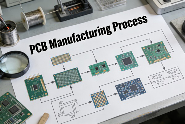
Table des matières
Aperçu du processus de fabrication des circuits imprimés
Bien que la complexité des circuits imprimés puisse varier, la plupart des circuits imprimés rigides suivent le même processus de fabrication :
- Fabrication de la couche interne
- Alignement et laminage des couches
- Forage
- Placage de cuivre
- Imagerie et gravure de la couche externe
- Application du masque de soudure
- Finition de la surface
- Sérigraphie
- Essais électriques et inspection finale
Chaque étape a une incidence directe sur la qualité, le rendement et coût.
Étape 1 - Fabrication de la couche intérieure
Imagerie de la couche interne
La fabrication commence par des feuilles laminées recouvertes de cuivre. Le modèle de circuit souhaité est transféré sur la surface du cuivre à l'aide d'une résine photosensible et d'une exposition aux UV.
Facteurs clés :
- Précision de la largeur de la trace et de l'espacement
- Précision de l'alignement des photos
- Environnement en salle blanche
Gravure de la couche interne
Le cuivre non désiré est éliminé par attaque chimique, laissant les traces de circuit nécessaires.
Du point de vue de la fabrication :
- Des traces plus fines augmentent la difficulté de la gravure
- Le surmordançage ou le sous-mordançage affecte le rendement
Chez TOPFAST, les paramètres de gravure de la couche interne sont optimisés pour équilibrer précision et stabilité de la production.
Étape 2 - Alignement des couches et laminage
Pour les circuits imprimés multicouches, les couches internes sont empilées avec des feuilles de cuivre pré-imprégnées et externes.
Processus de laminage
- La chaleur et la pression lient toutes les couches entre elles
- L'alignement précis assure des connexions via précises
Impact sur les coûts et la qualité :
- La multiplication des couches augmente les cycles de laminage
- Le laminage séquentiel augmente la complexité et le coût
Étape 3 - Perçage
Le perçage permet de créer des trous pour les vias et les fils des composants.
Forage mécanique
Utilisé pour :
- Orifices de passage
- Trous de plus grande taille
Le coût du forage augmente avec :
- Diamètres de trous plus petits
- Ratios d'aspect plus élevés
- Nombre élevé de forages
Perçage au laser (circuits imprimés avancés)
Le perçage au laser est utilisé pour :
- Microvias dans les circuits imprimés HDI
Ce processus nécessite un équipement spécialisé et augmente le coût de fabrication.
Étape 4 - Placage du cuivre
Après le perçage, les trous doivent être électriquement conducteurs.
Dépôt de cuivre chimique
Une fine couche de cuivre est déposée à l'intérieur des trous percés pour permettre une connexion électrique entre les couches.
Placage électrolytique
Du cuivre supplémentaire est plaqué pour :
- Renforcer les vias
- Atteindre l'épaisseur de cuivre requise
L'uniformité du placage a une incidence directe sur la fiabilité, en particulier pour les applications à courant élevé ou à haute fiabilité.
Étape 5 - Imagerie et gravure de la couche externe
Le circuit de la couche externe est formé selon un processus similaire à celui des couches internes.
Principaux défis :
- Maintien de la précision des traces après le placage
- Contrôle de l'épaisseur du cuivre
- Prévention des courts-circuits ou des ouvertures
Le traitement de la couche extérieure a un impact majeur sur rendement final.
Étape 6 - Application du masque de soudure
Objectif du masque de soudure
Masque de soudure :
- Protège les traces de cuivre
- Empêche les ponts de soudure
- Améliore l'isolation électrique
Les couleurs courantes sont le vert, le noir, le bleu et le rouge. Le vert reste l'option la plus rentable et la plus utilisée.
Facteurs de qualité du masque de soudure
- Exactitude de l'enregistrement
- Epaisseur du masque
- Définition de l'ouverture
Un masque de soudure de mauvaise qualité peut entraîner des défauts d'assemblage ultérieurs.
Étape 7 - Finition de la surface
La finition de la surface protège les pads de cuivre exposés et assure la soudabilité.
Options courantes de finition de surface
- HASL: Rentable, largement utilisé
- ENIG: Surface plane, plus grande fiabilité
- OSP: Faible coût, durée de conservation limitée
TOPFAST recommande des finitions de surface basées sur les exigences de l'application plutôt que les préférences par défaut.
Étape 8 - Sérigraphie
La sérigraphie ajoute :
- Désignateurs de référence des composants
- Marques de polarité
- Logos ou identifiants
Bien qu'elle ne soit pas électriquement fonctionnelle, une sérigraphie claire améliore la précision de l'assemblage et la maintenance.
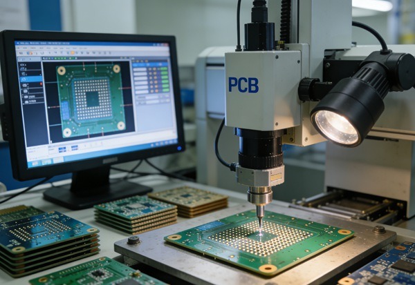
Étape 9 - Essais électriques et inspection finale
Essais électriques
Les essais électriques permettent de vérifier :
- Continuité
- L'isolement
- Absence de short et d'ouverture
Cette étape est essentielle pour garantir la fiabilité du fonctionnement.
Inspection finale de la qualité
L'inspection finale peut comprendre
- Inspection visuelle
- AOI (Inspection optique automatisée)
- Contrôles dimensionnels
Chez TOPFAST, les normes d'inspection sont alignées sur Exigences de l'IPC et les spécifications du client.
Comment le processus de fabrication des circuits imprimés influe sur le coût et la qualité
Chaque étape de la fabrication est introduite :
- Variabilité des processus
- Considérations relatives au rendement
- Implications financières
Les facteurs de coût les plus courants sont les suivants :
- Nombre élevé de couches
- Petites tailles de forets
- Tolérances serrées
- Finitions de surface avancées
La compréhension de l'ensemble du processus permet aux concepteurs de optimiser la conception des circuits imprimés en termes de coût et de fabricabilité.
Point de vue d'un fabricant : comment TOPFAST optimise la fabrication des circuits imprimés
En tant que fabricant de circuits imprimés, TOPFAST se concentre sur.. :
- Normalisation des processus
- Retour d'information précoce sur la DFM
- Prise de décision axée sur le rendement
- Une production stable et évolutive
Plutôt que d'imposer des processus avancés inutiles, TOPFAST met l'accent sur les points suivants des conceptions adaptées à la fabrication qui garantissent une qualité constante.
Conclusion
Le processus de fabrication des PCB est une séquence d'étapes soigneusement contrôlées, chacune contribuant aux performances, à la fiabilité et au coût de la carte finale.
En comprenant comment les circuits imprimés sont fabriqués - de la fabrication de la couche interne à l'inspection finale - les ingénieurs et les acheteurs peuvent prendre de meilleures décisions en matière de conception et d'approvisionnement.
Avec une approche axée sur la fabrication, TOPFAST aide les clients à transformer des conceptions complexes en circuits imprimés fiables et rentables..
FAQ sur le processus de fabrication des PCB étape par étape
R : La fabrication d'un circuit imprimé standard prend généralement de 5 à 10 jours ouvrables, en fonction de la complexité et de la quantité.
R : Chaque étape est importante, mais le perçage et la métallisation sont essentiels pour la fiabilité électrique.
R : Oui. Les circuits imprimés multicouches nécessitent des étapes supplémentaires de laminage et d'alignement.
R : Oui. Les conceptions alignées sur les capacités de fabrication améliorent le rendement et réduisent les coûts.
R : TOPFAST utilise des processus standardisés, un examen DFM et une inspection complète pour garantir une qualité constante.