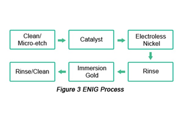
ENIG (elektrolytisch nikkel-immersie-goud) proces
In de PCB productieprocesDe oppervlaktebehandeling speelt een doorslaggevende rol in de prestaties, betrouwbaarheid en levensduur van het eindproduct. Als een van de populairste oplossingen voor PCB-oppervlaktebehandeling vandaag de dag, is elektroless nickel immersion gold (ENIG) de voorkeur geworden voor veel high-end elektronische producten vanwege de uitstekende uitgebreide prestaties.
Inhoudsopgave
Wat is het ENIG-proces?
ENIG (Electroless Nickel Immersion Gold) is een oppervlaktebehandelingsproces dat een nikkel-fosforlegeringslaag afzet op het oppervlak van koperen pads met chemische middelen, gevolgd door een verdringingsreactie om een dunne goudlaag af te zetten. Deze tweelagige structuur zorgt voor uitstekende soldeerprestaties en een superieure oxidatiebescherming.
Procesprincipe en structurele kenmerken van ENIG
Het ENIG-proces bestaat uit twee hoofdstappen: elektrolytisch vernikkelen en goud onderdompelen.
Ten eerste vormt zich bij chemisch vernikkelen een nikkel-fosforlegeringslaag (Ni-P) op het koperoppervlak. Deze laag is meestal 4-8 μm dik, met een fosforgehalte tussen 7-11%. Deze amorfe nikkellaag fungeert als een sterke diffusiebarrière en een solide basis voor solderen.
Vervolgens wordt tijdens de onderdompelingsgoudstap een zuivere goudlaag van 0,05-0,15 μm bovenop het nikkel aangebracht. Deze goudlaag voorkomt oxidatie van nikkel en zorgt voor een goede soldeerbaarheid.
Belangrijkste voordelen van het ENIG-proces
1. Uitzonderlijke soldeerbaarheid
De goudlaag vermengt zich snel met soldeer, waardoor vers nikkel zichtbaar wordt.Hierdoor ontstaan sterke Ni-Sn intermetallische verbindingen.
2.Uitstekende weerstand tegen oxidatie
De goudlaag houdt zuurstof en vocht effectief buiten.Dit zorgt ervoor dat de PCB soldeerbaar blijft tijdens opslag en verzending.
3.Goede vlakheid van het oppervlak
Chemisch aangebrachte coatings zorgen voor een glad oppervlak.Dit is perfect voor assemblage met hoge dichtheid en onderdelen met fijne pitch.
4.Betrouwbare hechtprestaties
Het nikkeloppervlak werkt goed voor het hechten van goud- en aluminiumdraad.Het voldoet aan de eisen van chip-schaal verpakking.
5.Uitgebreide dekkingsmogelijkheden
Het bedekt doorvoergaten, blinde vias en ingegraven vias gelijkmatig.Dit voldoet aan de eisen van interconnecties met een hoge dichtheid.
We zijn blij te kunnen aankondigen dat ons product RoHS-conform is!Het is geweldig om te weten dat het de milieuregels volgt en geen schadelijke stoffen bevat zoals lood, kwik of cadmium.
6.Voorkomen van kopermigratie
De nikkellaag voorkomt dat koper diffundeert in soldeerverbindingen.Dit voorkomt brosse intermetallische verbindingen.
We zijn verheugd onze betrouwbaarheid op lange termijn te kunnen presenteren!Verbazingwekkend genoeg blijft dit product stabiel presteren in omgevingen met hoge temperaturen en hoge vochtigheid. Het is perfect voor zelfs de zwaarste toepassingen.
Belangrijkste kwaliteitscontrolepunten voor ENIG-proces
Om de kwaliteit van het ENIG-proces te handhaven, moeten we verschillende belangrijke parameters controleren:
- Nikkel Laagdikte Controle: Dit moet tussen 4-8 μm blijven. Als het te dun is, kan er ‘zwart nikkel’ ontstaan. Als het te dik is, stijgen de kosten zonder dat dit voordelen oplevert.
- Fosfor Inhoudsbeheer: Houd het tussen 7-11%. Dit is essentieel voor corrosiebestendigheid en betrouwbaar solderen.
- Goudlaagdiktecontrole: Streef naar 0,05-0,1 μm. Een dunne laag biedt onvoldoende bescherming, terwijl een dikke laag de soldeerverbindingen kan verzwakken.
- Oplossing Onderhoud: Regelmatige controles en aanpassingen van de plateringsoplossing zorgen voor een stabiele afzettingssnelheid en een goede coatingkwaliteit.
- Kwaliteit voorbehandeling: Reinig en ruw het koperoppervlak goed op voor een sterke hechting.
Bij Topfast leveren we ENIG PCB's die voldoen aan de hoogste kwaliteitsnormen.Dit bereiken we door geautomatiseerde productie en strenge procescontrole voor onze klanten.
Vergelijking met andere PCB-oppervlaktebehandelingsprocessen
ENIG heeft veel voordelen, maar andere oppervlaktebehandelingsmethoden zijn nog steeds nuttig in bepaalde situaties.Hier zijn korte beschrijvingen van verschillende PCB oppervlaktebehandelingstechnologieën:
Hete lucht soldeer nivellering (HASL)
Hot Air Solder Leveling (HASL) is een oud en populair proces voor PCB-oppervlaktebehandeling.Hierbij wordt de printplaat in gesmolten soldeer gedompeld en worden hete luchtmessen gebruikt om overtollig soldeer te verwijderen, zodat er een gelijkmatige laag ontstaat.
Procesvoordelen:
- Kosteneffectief met stabiele technologie
- Produceert een dikke soldeerlaag voor meerdere reflow-cycli
- Biedt goede soldeerprestaties met diverse legeringen
- Repareert effectief kleine oppervlaktedefecten
HASL werkt goed voor kostengevoelige toepassingen met behoefte aan een lage vlakheid van het oppervlak, zoals consumentenelektronica, voedingsmodules en industriële besturingsborden. Naarmate de componenten echter kleiner worden, worden HASL’s vlakheidsproblemen opvallender.
Organisch soldeerbaarheidsbewaarmiddel (OSP)
OSP creëert een organische laag op schone koperen oppervlakken.Deze laag voorkomt dat koper oxideert bij kamertemperatuur. Tijdens solderen op hoge temperatuur breekt het snel af, waardoor het koper vrij komt om te solderen.
Procesvoordelen:
- Biedt uitstekende vlakheid en coplanariteit, ideaal voor componenten met een zeer fijne pitch.
- Eenvoudig en milieuvriendelijk, met gemakkelijke afvalwaterbehandeling.
- Kosteneffectief, slechts 30-50% van ENIG.
- Goede coplanariteit, geschikt voor componenten zoals BGA's en QFN's.
OSP werkt goed voor mobiele apparaten met een groot volume en consumentenelektronica met een hoge dichtheid. De beschermlaag is echter kwetsbaar, heeft een korte houdbaarheid en is niet ideaal voor meerdere soldeercycli. Ook beperkt dit het toepassingsgebied.
Dompelzilver ~4,3-4,8)
Bij onderdompeling wordt een dunne laag zilver op koper aangebracht. Dit gebeurt door middel van een chemische verplaatsingsreactie. De dikte van het zilver varieert gewoonlijk van 0,1 tot 0,4 μm.
Procesvoordelen:
- Uitstekende vlakheid en coplanariteit van het oppervlak.
- Goede soldeerprestaties, wat de betrouwbaarheid van soldeerverbindingen verbetert.
- Ideaal voor toepassingen met hoge frequenties; het hoge geleidingsvermogen van zilver’ verbetert de signaaloverdracht.
- Milieuvriendelijk, want vrij van halogenen en zware metalen.
Het dompelzilverproces is populair in communicatieapparatuur en digitale producten met hoge snelheid. Ontwerpers moeten echter rekening houden met zilvermigratie en verkleuring.
Dompelblik
Door middel van onderdompeling wordt een laag tin op koper aangebracht via een verplaatsingsreactie. De dikte varieert van 0,8 tot 1,5 μm, wat zorgt voor een vlak oppervlak en een goede soldeerbaarheid.
Procesvoordelen:
- Uitstekende vlakheid van het oppervlak, ideaal voor onderdelen met fijne pennen.
- Goede soldeerprestaties, voldoet aan loodvrije eisen.
- Gematigde kosten, tussen OSP en ENIG.
- Geschikt voor persverbindingen, met een harde tinlaag.
Dompeltin komt vaak voor in auto-elektronica en industriële besturing. Tingroei en een korte houdbaarheid zijn echter uitdagingen die zorgvuldig beheer vereisen.
Uitgebreide vergelijking van ENIG en andere oppervlaktebehandelingsprocessen
Vergelijking van PCB oppervlakteafwerkingen
| Evaluatie Dimensie | OSP | ENIG (Elektrolytisch Nikkel Onderdompelingsgoud) | Dompelzilver ~4,3-4,8) | Dompelblik | Hard verguld |
|---|---|---|---|---|---|
| Kosten | Meest kosteneffectief | Midden- tot hoog bereik | Matig | Matig | Hoogste |
| Technische prestaties | Goed voor eenvoudige toepassingen | Meest gebalanceerd, superieur voor high-end gebruik | Uitstekend voor hoogfrequente | Goed voor solderen & perspassing | Uitstekende slijtvastheid |
| Complexiteit van het proces | Eenvoudigste | Matig | Matig | Matig | Meest complex |
| Milieuvereisten | Meest milieuvriendelijk | Nikkel afvalwaterbehandeling vereist | Matig | Matig | Vereist complexe afvalverwerking |
| Typische toepassingen | Consumentenelektronica | Auto's, Betrouwbare elektronica | Toepassingen voor hoge frequenties/RF | Automobielindustrie, industriële besturing | Connectoren, gebieden met hoge slijtage |
Voordelen van het kiezen van Topfast’s ENIG-diensten
Als topfabrikant van printplaten blinkt Topfast uit in het ENIG-proces:
- Nauwkeurige procesbesturing: We gebruiken geautomatiseerde apparatuur voor een consistente laagdikte en kwaliteit.
- Strenge kwaliteitsinspectie: Ons kwaliteitscontrolesysteem controleert alles, van grondstoffen tot afgewerkte producten.
- Milieuvriendelijke behandeling: We hebben geavanceerde afvalwatersystemen die voldoen aan alle milieuvoorschriften.
- Snel reactievermogen: Wij bieden flexibele productie en snelle monsterdiensten.
- Technische ondersteuningOns vakkundig technisch team adviseert de beste oplossingen voor oppervlaktebehandeling.
Of u nu ENIG, OSP, onderdompeling in zilver of andere speciale behandelingen nodig hebt, Topfast biedt betrouwbare opties. Neem contact op met ons technisch team voor meer informatie. Wij helpen u bij het kiezen van de beste oppervlaktebehandeling voor uw behoeften.


Verwante berichten