Разработка и производство 16-слойных печатных плат
16-слойные печатные платы (ПП) стали ключевым технологическим носителем для комплексной системной интеграции. Их разработка и производство предполагают точный межслойный контроль и управление целостностью сигнала. Эти многослойные платы идеально сочетают требования к высокой плотности проводки и целостности сигнала благодаря точной многослойной структуре.
Ii. Содержание
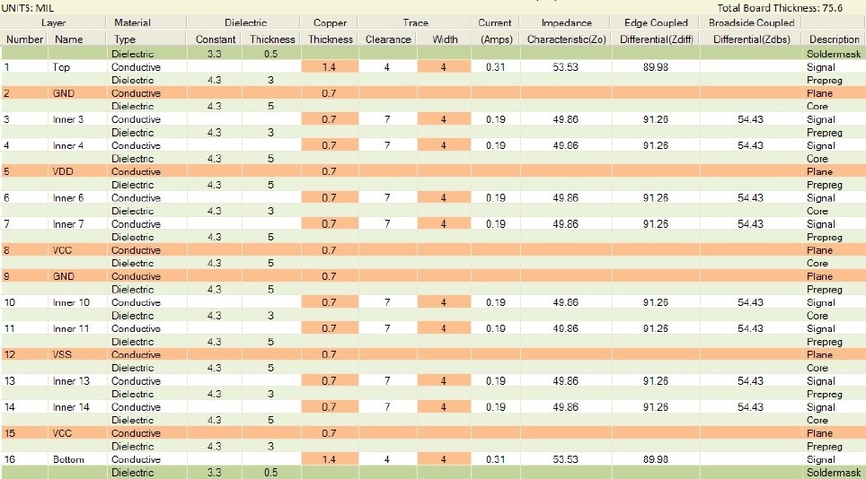
Типичная структура ламината 16-слойной печатной платы
Конфигурация 1: Оптимизированный высокоскоростной сигнал (8S4P4G)
L1: Сигнал(TOP) L2: GND L3: Сигнал L4: Сигнал
L5: PWR1 L6: GND L7: Сигнал L8: Сигнал
L9: PWR2 L10:GND L11:Сигнал L12:Сигнал
L13:PWR3 L14:GND L15:Сигнал L16:GND(BOT)Преимущества:
- Каждый сигнальный слой имеет смежную опорную плоскость
- Раздельные плоскости питания позволяют использовать несколько доменов напряжения
- Подходит для высокоскоростных последовательных линий 56 Гбит/с+
Конфигурация 2: тип обработки смешанных сигналов
L1: Радиочастотный сигнал L2: GND L3: Analog L4: PWR
L5: Цифровой L6: GND L7: Цифровой L8: PWR
L9: Цифровой L10:GND L11:Цифровой L12:PWR
L13:Аналоговый L14:GND L15:RF L16:GND
Особенности сайта:
- Радиочастотные и аналоговые схемы с экранированием по периметру
- Цифровая маршрутизация сигналов на внутренних слоях
- Идеально подходит для медицинского оборудования для визуализации
Конфигурация 3: Тип приложения высокой мощности
(Включая силовые слои из меди толщиной 2 унции и специальные тепловые слои)Ключевые моменты:
- 3OZ толстые медные силовые слои
- Встраиваемые тепловые слои с металлическим сердечником
- Предназначен для инверторов EV
Рекомендация эксперта: Проведите трехмерное моделирование электромагнитного поля при выборе конфигурации стека. Для проверки конструкции рекомендуется использовать Ansys HFSS или CST Studio Suite.
Технология критических материалов и контроль толщины
1. Выбор высококачественных материалов
| Тип материала | Типовая модель | Dk@10 ГГц | Df@10 ГГц | Приложения |
|---|---|---|---|---|
| Высокоскоростной FR4 | Мегатрон 6 | 3.7 | 0.002 | 112 Гбит/с SerDes |
| Материал с низким уровнем потерь | RO4835 | 3.5 | 0.003 | Радар на миллиметровых волнах |
| Материал с высоким содержанием тг | IT-180A | 4.3 | 0.012 | Автомобильная электроника |
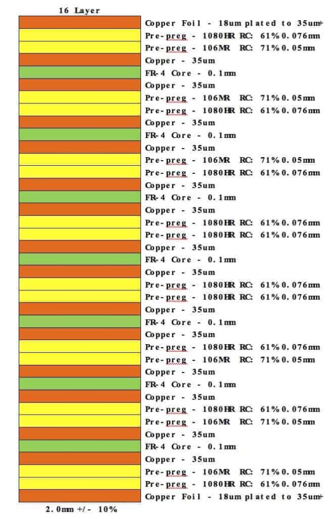
2.Система контроля толщины
Пример для толщины доски 1,6 мм:
- Медь сигнального слоя: 1 унция (35 мкм)
- Медный слой питания: 2 унции (70 мкм)
- Толщина диэлектрика: 0,1 мм (4 мил)
- Препрег: 1080 тип
- Слой контроля импеданса: 0,2 мм (8 мил)
Формула расчета:
Общая толщина = Σ(толщина меди) + Σ(толщина диэлектрика) + толщина паяльной маски
Технологический процесс передового производства
- Технология лазерного сверления:
- CO2-лазер: отверстия >100 мкм
- УФ-лазер: микроотверстия менее 100 мкм
- Слепой через соотношение сторон: 1:0,8
- Импульсный процесс нанесения покрытия:
- Толщина медного слоя отверстия: ≥25 мкм
- Равномерность поверхности меди: ±3 мкм
- Точность обратногосверления: ±50 мкм
- Критические параметры ламинирования:
- Температура:180±5℃
- Давление: 350PSI
- Продолжительность: 90 минут
- Уровень вакуума: <50 мбар
Стандарты проверки качества:
- IPC-6012B Класс 3
- IPC-A-600G
- 100% испытание летающего зонда
- 3D рентгеновский контроль
Распределение сигнальной целостностиПитание модуля:
- Три элемента импедансного контроля:
- Допуск по ширине линии ±10%
- Допуск по толщинедиэлектрика ±7%
- Допуск по толщинемеди ±1 мкм
- Проектирование целостности электропитания:
- Плоская емкость >500 пФ/дюйм²
- Размещение развязывающих конденсаторов:
- 0,1 мкФ@0402на BGA
- 10мкФ@0603 на область напряжения
- Стратегии оптимизации EMC:
- Экранирующиепереходные отверстия: расстояние <λ/20
- Изоляционныепазы:ширина >50 мил
- Многослойная конструкция основания
Деловое исследование: Базовая станция 5G AAU с использованием 16-слойных печатных плат достигла 32 % меньших вносимых потерь, 28 % лучших тепловых характеристик и надежности 100 000 часов MTBF.
Рекомендуемые профессиональные производственные услуги
3. Топфаст предлагает 16-слойные печатные платы премиум-класса под ключ:
✅ До 32-слойной настраиваемой сборки
✅ Контроль импеданса ±5%
✅ 100 мкм лазерныеслепые переходные отверстия
✅ Быстрые прототипы, напечатанные на 3D-принтере
✅ Полный спектр услуг по моделированию SI/PI
Получите мгновенное индивидуальное предложение: Предоставление технических требований
Основные моменты FQA
Вопрос: Как сбалансировать стоимость и производительность в 16-слойных конструкциях?
О: Рекомендуется “4+8+4” гибридное ламинирование: 4 слоя высокоскоростного материала + 8 слоев FR4 снижают стоимость на 15% при сохранении критических характеристик сигнального слоя.
Вопрос: Как решить тепловые проблемы в 16-слойных платах?
О: Три эффективных решения:
- Встроенные медные блоки для локального охлаждения
- Термические решетки
- Композитные материалы с металлическим сердечником
Вопрос: Распространенные дефекты при массовом производстве 16-слойных плат?
О: Ключевые направления:
- Перекос между слоями
- Медные трещины в каналах
- Пустоты в диэлектрических слоях
- Неравномерная обработка поверхности
Области применения 16-слойных печатных плат
16-слойные печатные платы идеально сочетают в себе высокую плотность маршрутизации и требования к целостности сигнала благодаря точной структуре укладки, находя широкое применение в:
- Инфраструктура связи 5G: Оборудование базовых станций с поддержкой передачи данных в миллиметровых волнах и технологии массивного MIMO
- Высокопроизводительные вычисленияПроцессорные межсоединения для серверов и суперкомпьютеров искусственного интеллекта
- Оборудование для медицинской визуализации: Системы управления для КТ, МРТ и других современных медицинских приборов
- Аэрокосмическая электроника: Надежные решения для спутниковой связи и систем управления полетом
- Автомобильная электроникаКонтроллеры домена для систем автономного вождения и интеллектуальной кабины пилота
Типовые технические параметры:
- Толщина доски: 1,6-2,4 мм (настраивается)
- Минимальная ширина линии/расстояния: 3/3mil (0.075/0.075mm)
- Минимальное отверстие:0,15 мм (лазерное сверление)
- Допуск по выравниванию слоев: ±25 мкм
- Точность регулирования импеданса: ±7%
Отраслевой обзор: С принятием технологий PCIe 5.0 и DDR5 рынок 16-слойных печатных плат растет на 12 % в год и, по прогнозам, к 2025 году превысит 5,8 млрд долларов США.
Проконсультируйтесь с нашими экспертами прямо сейчас: Скачать 16-слойную печатную плату
Рекомендации по чтению
4-слойная гибкая печатная плата
Проектирование и производство 6-слойной укладки печатных плат


Похожие посты