Травление - это процесс, при котором превращает плакированную медь в точные схемы.
Хотя на первый взгляд все выглядит просто, травление является одним из наиболее чувствительные к урожайности этапы в производстве печатных плат.
С точки зрения производителя, плохой контроль травления приводит к:
- Изменение ширины линии
- Шорты и отверстия
- Низкая урожайность
- Более высокая стоимость производства
В этой статье рассказывается о том, как работает травление печатных плат, что влияет на качество травления и как производители, такие как 3. Топфаст контроль выхода продукции для обеспечения стабильного и экономически эффективного производства печатных плат.
Ii. Содержание
Что такое травление печатных плат?
Травление печатных плат - это химический процесс, который удаляет нежелательную медь с платы, оставляя только разработанную схему.
Травление применяется для:
- Внутренние слои
- Внешние слои
Цель - достичь точная ширина, расстояние между трассами и геометрия в соответствии с проектными спецификациями.
Типы процессов травления печатных плат
Травление внутреннего слоя
Происходит травление внутреннего слоя:
- Перед ламинированием
- На тонкой медной фольге
Он очень чувствителен, потому что:
- Дефекты не могут быть устранены после ламинирования
- Выход внутреннего слоя влияет на весь стек печатной платы
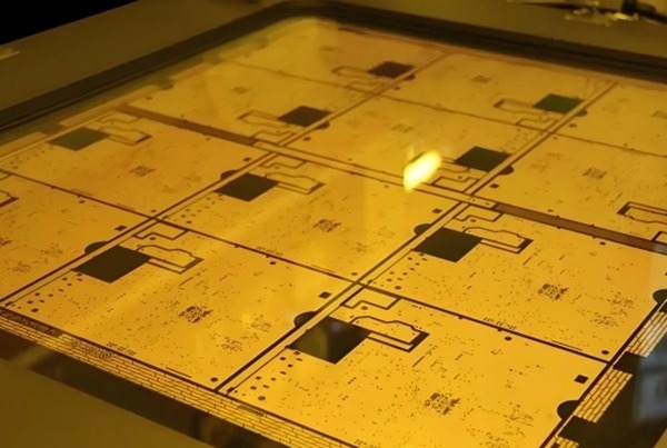
Травление наружного слоя
Происходит травление наружного слоя:
- После медного покрытия
- На более толстых медных слоях
Травление наружного слоя должно учитывать:
- Толщина медного покрытия
- Равномерность по всей панели
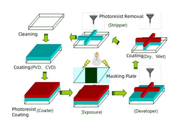
Пошаговый процесс травления печатных плат
Шаг 1 - Подготовка узора для резиста
Слой резиста защищает медные участки, которые должны остаться после травления.
Точность детали на этом этапе определяет окончательную геометрию трассы.
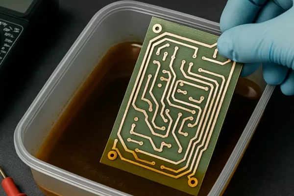
Шаг 2 - Химическое травление
Химические растворы избирательно удаляют обнаженную медь.
Ключевые переменные процесса:
- Концентрация протравителя
- Температура
- Давление распыления
- Время травления
Контроль над этими переменными необходим для получения стабильных результатов.
Шаг 3 - сопротивление полосканию
После травления остатки резиста удаляются, обнажая готовые медные трассы.
Распространенные дефекты травления и их влияние
Надглазурная гравюра
Причины:
- Чрезмерное время травления
- Агрессивная химия
Результаты:
- Уменьшение ширины трассы
- Увеличенный импеданс
- Потенциал открывается
Подтравка
Причины:
- Недостаточное время травления
- Слабая активность травителя
Результаты:
- Остаточная медь
- Короткие замыкания между трассами
Подрезка
Травление удаляет медь в боковом направлении под резистом, уменьшая ширину трассы.
Подрезание становится все более сильным:
- Более толстая медь
- Более тонкие трассировки
Что такое выход в производстве печатных плат?
Урожайность относится к процент досок, соответствующих спецификациям после изготовления.
Высокая доходность означает:
- Более низкая стоимость единицы продукции
- Стабильное качество
- Предсказуемая доставка
Низкая доходность приводит к:
- Лом
- Переработка
- Более высокая общая стоимость
Как травление влияет на производительность
Травление напрямую влияет на урожайность, поскольку:
- Дефекты трассировки вызывают электрический сбой
- Дефекты внутреннего слоя увеличиваются во всех панелях
- Небольшие отклонения влияют на конструкции высокой плотности
С точки зрения производителя, травление является одним из самые высокие точки опоры для повышения урожайности.
Факторы проектирования, влияющие на выход травления
Урожайность повышается при разработке дизайна:
- Избегайте излишне тонких следов
- Поддерживайте постоянную ширину линии
- Распределение балансовой меди
- Используйте рекомендованные производителем минимальные расстояния
DFM обзор часто позволяет выявить риски, связанные с травлением, на ранней стадии.
Как производители контролируют выход травления
Мониторинг процессов
Ключевые элементы управления включают:
- Непрерывный химический анализ
- Калибровка оборудования
- Измерение ширины линии в режиме реального времени
Оптимизация на уровне панели
Производители оптимизируют:
- Расположение панелей
- Медный баланс
- Равномерность травления по всей панели
Проверка и отзывы
AOI и электрические испытания обеспечивают обратную связь:
- Настройка параметров травления
- Повышение стабильности процесса
В компании TOPFAST данные о выходе продукции активно используются для совершенствования процессов травления и предотвращения повторных проблем.
Влияние травления и потери урожайности на стоимость
Низкая урожайность увеличивает стоимость из-за:
- Лом материалов
- Дополнительные трудозатраты
- Задержки в производстве
Повышение производительности травления часто оказывается более эффективным, чем стоимость режущего материала при снижении стоимости печатной платы.
Перспективы производителя: Стратегия травления TOPFAST, ориентированная на доходность
TOPFAST контролирует выход травления:
- Стандартизированные технологические окна
- Консервативные рекомендации по проектированию
- Обратная связь на ранних этапах DFM
- Непрерывный контроль урожайности
Основное внимание уделяется стабильное качество и масштабируемое производствоНе просто соблюдение минимальных допусков.
Iii. Выводы и рекомендации
Травление печатных плат - это обманчиво простой процесс с существенно влияет на урожайность, стоимость и надежность.
Понимая, как работает травление и что влияет на выход продукции, дизайнеры и покупатели могут принимать более разумные решения:
- Снижение производственных рисков
- Снижение общей стоимости
- Повышение надежности продукции
Благодаря производственному подходу, ориентированному на выход продукции, 3. Топфаст обеспечивает стабильное качество травления, что способствует надежному производству печатных плат в промышленных масштабах.
Related Reading
Процесс производства печатных плат Процесс производства печатных плат
Изготовление внутреннего слоя печатной платы
Сверление печатных плат в сравнении с лазерным сверлением
Процесс нанесения медного покрытия
FAQ по контролю урожайности травления
О: Травление печатных плат - это химический процесс, в ходе которого удаляется ненужная медь для формирования рисунка схемы.
О: Чрезмерное травление вызвано чрезмерным временем травления или слишком агрессивными химическими растворами.
О: Плохой контроль травления приводит к появлению дефектов трассировки, что снижает выход продукции и увеличивает затраты.
О: Да. Конструкции с разумной шириной трасс и расстоянием между ними значительно повышают производительность травления.
О: TOPFAST использует стандартизированные процессы, мониторинг в реальном времени и обратную связь с DFM для поддержания стабильной производительности травления.