Производственные дефекты печатных плат редко бывают случайными.
Большинство дефектов возникает из-за конструкторские решения, ограничения по материалу или нестабильность процессазадолго до проведения окончательной проверки.
При осмотре можно обнаружить множество видимых проблем, предотвращение дефектов должно происходить на более ранних этапах производственного процесса.
В этой статье рассказывается о наиболее распространенных дефектах при производстве печатных плат, их основных причинах и практических стратегиях предотвращения с точки зрения производства.
Об основах качества см: Что определяет качество печатной платы?
Ii. Содержание
Что считается производственным дефектом печатной платы?
Производственный дефект печатной платы - это любое отклонение, которое:
- Влияет на электрические характеристики
- Нарушает механическую целостность
- Снижение долгосрочной надежности
- Нарушает спецификации IPC или заказчика
Дефекты могут быть видимый, латентный, или прогрессивныйПоявляются только после термического или механического воздействия.
Дефекты внутреннего слоя
Распространенные дефекты внутреннего слоя
- Разомкнутые цепи
- Короткие замыкания
- Перетравливание или недотравливание
- Неправильная регистрация между слоями
Коренные причины
- Неточности при визуализации
- Вариации процесса травления
- Плохое выравнивание внутреннего слоя
Поскольку внутренние слои запечатываются во время ламинирования, дефекты на этом этапе необратимый.
Предыстория процесса: Изготовление внутреннего слоя: объяснение
Дефекты, связанные с бурением
Типичные дефекты при сверлении
- Отверстия со смещенным центром
- Заусенцы и мазки
- Сломанные сверла
- Низкое качество стенок отверстия
Коренные причины
- Чрезмерное соотношение сторон сверла
- Изношенная оснастка
- Неправильная подача и скорость
- Неправильный метод бурения
Дефекты сверления напрямую влияют на качество медного покрытия и надежность работы системы.
Сравнение методов:
Сверление печатных плат в сравнении с лазерным сверлением
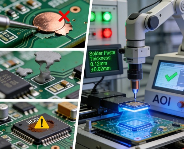
Дефекты покрытия
Общие проблемы с покрытием
- Тонкая медь в проходах
- Пустоты или пробелы
- Шероховатая или ноздреватая медь
- Плохая адгезия
Коренные причины
- Неправильная подготовка поверхности
- Непостоянная плотность тока
- Химический дисбаланс
- Проходы с высоким аспектным отношением
Дефекты покрытия являются одной из основных причин периодические сбои и проблемы с термоциклированием.
Детали процесса: Процесс нанесения медного покрытия при производстве печатных плат
Дефекты травления
Типичные дефекты травления
- Затравленные следы
- Медные мостики с неполным протравливанием
- Изменение ширины линии
- След на шее
Коренные причины
- Неравномерная толщина меди
- Агрессивный химический состав травителя
- Плохая компенсация процесса
- Малое расстояние между трассами
По мере того как геометрия трассировки становится все более тонкой, дефекты травления все больше влияют на производительность и надежность.
Анализ, ориентированный на доходность: Процесс травления печатных плат и контроль выхода продукции
Дефекты ламинирования и расслоения
Распространенные проблемы ламинирования
- Расслаивание
- Blistering
- Пустоты в смоле
- Смещение слоев
Коренные причины
- Неправильное давление или температура ламинирования
- Плохой выбор препрега
- Поглощение влаги
- Несбалансированные штабеля
Эти дефекты часто проявляются во время сборки или термоциклирования, а не во время первоначальных испытаний.
Материальные отношения: Стоимость материалов и слоев печатной платы
Дефекты паяльной маски и шероховатости поверхности
Типичные дефекты
- Перекос паяльной маски
- Плохая адгезия
- Дыроколы
- Неравномерная толщина поверхности
Коренные причины
- Недостаточная подготовка поверхности
- Неправильные условия отверждения
- Загрязнение процесса
Эти дефекты могут привести к образованию мостиков припоя, коррозии и сокращению срока годности.
Побеги при электрических испытаниях и скрытые дефекты
Не все дефекты обнаруживаются при электрическом тестировании.
Скрытые дефекты могут:
- Пройдите первоначальные испытания
- Выход из строя после термического воздействия
- Появляются во время работы в полевых условиях
К распространенным причинам относятся:
- Предельная толщина покрытия
- Микротрещины в проходах
- Формирование CAF
Риски, связанные с дефектами конструкции
Некоторые дефекты возникают из-за выбора конструкции, а не из-за производственных ошибок.
К факторам повышенного риска относятся:
- Исключительно тонкие следы и интервалы
- Проходы с высоким аспектным отношением
- Несбалансированное распределение меди
- Слишком жесткие допуски
Качественное соединение: Факторы стоимости проектирования печатных плат
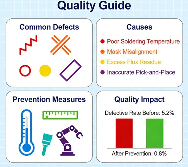
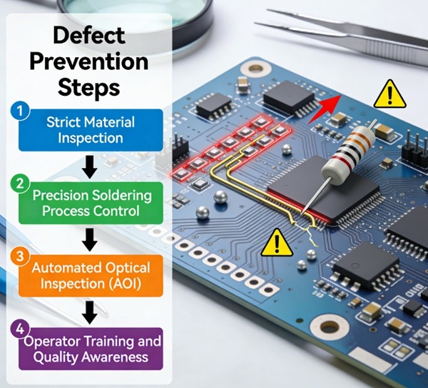
Как предотвратить дефекты при производстве печатных плат
Эффективное предотвращение дефектов направлено на стабильность процессаНе только осмотр.
Основные стратегии профилактики включают:
- Ранний обзор DFM
- Консервативные пределы проектирования
- Выбор квалифицированных материалов
- Мониторинг возможностей процесса
- Анализ данных об урожайности
В компании TOPFAST предотвращение дефектов определяется управление технологическими процессами и обратная связь на основе данныхЭто снижает зависимость от конечного скрининга.
Предотвращение дефектов в сравнении с затратами на производство
Предотвращение дефектов часто снижает общую стоимость.
Преимущества включают:
- Более высокая доходность
- Меньше переделок
- Меньше задержек
- Снижение риска выхода из строя месторождения
Баланс цены и качества: Стоимость производства печатной платы объясняется
Iii. Выводы и рекомендации
Производственные дефекты печатных плат редко бывают единичными случаями.
Они являются результатом взаимодействие между дизайном, материалами и управлением процессом.
Понимая распространенные типы дефектов и их основные причины, инженеры и покупатели могут предпринять упреждающие шаги для предотвращения дефектов и повышения долгосрочной надежности.
Эта статья составляет основу Качество и надежность печатных плат кластер.
ВОПРОСЫ И ОТВЕТЫ: Дефекты при производстве печатных плат
О: Дефекты, связанные с травлением, и проблемы с гальваническим покрытием - одни из самых распространенных.
О: Нет. Инспекция выявляет дефекты, но не предотвращает их первопричины.
О: Тепловое напряжение при сборке может выявить скрытые дефекты, возникшие ранее.
О: Нет. Многие дефекты возникают из-за дизайна или выбора материала.
О: С помощью анализа DFM и консервативного проектирования, согласованного с возможностями процесса.