Какова структура ламинирования печатных плат HDI?
Ii. Содержание
Структура ламинирования печатных плат HDI
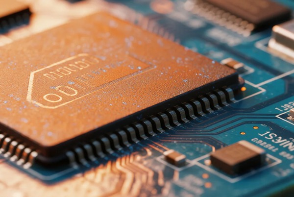
Смартфоны становятся все более тонкими, а смарт-часы - все более мощными. HDI (High-Density Interconnect) Технология печатных плат лежит в основе этой тенденции. По сравнению с традиционными печатными платами, конструкция ламинированной структуры HDI позволяет размещать более сложные схемы на меньшей площади.
Как производитель печатных плат с 17-летним опытом работы, компания Topfast стала свидетелем того, как множество проектов провалилось из-за выбора неподходящей структуры ламинирования HDI, что привело к превышению расходов или снижению производительности. Поэтому очень важно понимать различные структуры ламинирования печатных плат HDI.
1. Основы ламинирования печатных плат HDI
Суть HDI-плат заключается в достижении высокой плотности маршрутизации за счет процессы наращиваниякоторые в корне отличаются от традиционного производства печатных плат. Традиционные печатные платы похожи на изготовление сэндвичей - все слои ламинируются сразу, в то время как платы HDI напоминают строительство небоскребов, требующее многослойной конструкции.
Сравнение ключевых процессов:
- Лазерное сверление: Создает микропроходы диаметром до 0,05 мм (человеческий волос ≈ 0,07 мм)
- Импульсное покрытие: Обеспечивает равномерную толщину меди в микропроходах (разброс <10%)
- Последовательное ламинирование: Типичные параметры-170°C±2°C, давление 25 кг/см², послойное наращивание
В проекте смарт-часов, над которым я работал, переход от традиционной 6-слойной печатной платы (5 см²) к структуре HDI (1+4+1) позволил уменьшить размер платы до 1,5 см², добавив при этом функцию мониторинга сердечного ритма, что демонстрирует магию HDI.
Бесплатный обзор дизайна HDI →
2. Подробный анализ основных структур ламинирования HDI
1. Простое одинарное ламинирование (1+N+1)
Типичный пример: (1+4+1) 6-слойная плата
Особенности сайта:
- Отсутствие заглубленных отверстий во внутренних слоях, однослойное покрытие
- Слепые отверстия, сформированные лазерным сверлением на внешних слоях
- Самое экономичное решение HDI
Приложения:
- Смартфоны начального уровня
- Конечные устройства IoT
- Потребительская электроника с ограниченным пространством
Деловое исследование: Bluetooth-наушники с дизайном (1+4+1), объединяющим Bluetooth 5.0, сенсорное управление и управление батареей в пространстве диаметром 8 мм.
2. Стандартный однослойный HDI (с заглубленными отверстиями)
Типичный пример: (1+4+1) 6-слойная плата (заглубленные перегородки в L2-5)
Особенности сайта:
- Заглубленные проходы во внутренних слоях требуют двух ламинирований
- Комбинирует глухие и заглубленные проходы
- Сбалансированная стоимость и производительность
Ошибки в дизайне: Неправильное размещение заглубленных сквозных отверстий привело к отклонению импеданса 15% в одном проекте, что потребовало перепроектирования.
3. Стандартная двойная ламинация HDI
Типичный пример: (1+1+4+1+1) 8-слойная плата
Характеристики процесса:
- Три этапа ламинирования (сердцевина + первый слой + второй слой)
- Позволяет создавать сложные архитектуры межсоединений
- Поддержка трехступенчатых глухих проходов
Преимущества производительности:
- Подходит для высокоскоростных сигналов ГГц+
- Улучшенная целостность питания (выделенные уровни питания)
- 30% улучшенные тепловые характеристики
4. Оптимизированная структура двойного ламинирования
Инновационный дизайн: (1++1+4+1+1) 8-слойная плата
Основные усовершенствования:
- Перемещение заглубленных проходов с L3-6 на L2-7
- Исключение одного этапа ламинирования
- 15% снижение затрат
Данные испытаний: С помощью этой структуры был создан модуль 5G:
- Вносимые потери 0,3 дБ/см @10 ГГц
- 12% более низкая стоимость производства по сравнению с традиционными конструкциями
- 8% повышенная производительность
3. Усовершенствованные конструкции структуры ламинирования HDI
1. Дизайн Skip-Via
Технические проблемы:
- Слепые витки от L1 до L3, пропуская L2
- 100% увеличенная глубина лазерного сверления
- Значительно более твердое покрытие
Решения:
- Комбинированное УФ+CO₂ лазерное сверление
- Специальные добавки для глубоких отверстий
- Улучшенная оптическая юстировка (точность <25 мкм)
Извлеченный урок: Партия контроллеров для беспилотных летательных аппаратов вышла из строя из-за проблем с покрытием skip-via, что привело к затратам на доработку в размере $50 тыс.
2. Дизайн со стеком
Особенности сайта:
- Слепые проходы укладываются непосредственно над заглубленными проходами
- Более короткие вертикальные межсоединения
- Уменьшение точек отражения сигнала
Основы дизайна:
- Строгий контроль выравнивания слоев (погрешность <25 мкм)
- Закупорка смолой для предотвращения образования воздушных карманов
- Дополнительное испытание на термическую нагрузку (260°C, 10 с, 5 циклов)
4. Выбор структуры ламинирования HDI
1. Ключевые факторы выбора
| Рассмотрение | Простая одинарная ламинация | Сложная двойная ламинация |
|---|---|---|
| Расходы по проекту | $ | $$$ |
| Плотность маршрутизации | Средний | Чрезвычайно высокий |
| Целостность сигнала | Подходит для работы на частоте <1 ГГц | Подходит для работы на частоте >5 ГГц |
| Время разработки | 2-3 недели | 4-6 недель |
| Ставка доходности | >90% | 80-85% |
2. Рекомендации для конкретной отрасли
Потребительская электроника:
- Предпочтение: (1+4+1)
- След/пространство: 3/3mil
- Слепое отверстие: 0,1 мм
Автомобильная электроника:
- Рекомендуемые: (1+1+4+1+1)
- Материал: TG≥170°C
- Дополнительные тепловые каналы
Медицинское оборудование и принадлежности:
- Высочайшие требования к надежности
- Закупорка смолой с низким содержанием пустот
- 100% микросекционный контроль
5. Практические методы проектирования ИЧР
1. Принципы оптимизации
- ≤3 Пазы в высокоскоростных сигнальных трактах
- Расстояние между соседними отверстиями ≥5× диаметр отверстия
- Двойные силовые провода
2. Золотые правила Stack-Up
- Сигнальные слои, прилегающие к земляным плоскостям
- Внутренняя прокладка высокоскоростных сигналов (уменьшает излучение)
- Жесткая связь между плоскостью питания и землей
3. Повышение надежности
- Добавьте 0,1-миллиметровые тепловые каналы
- Наземные ограждения для критических сигналов
- 0,5 мм зона отсутствия фрезеровки на краях платы
6. Тенденции будущего
Новые технологии:
- Модифицированный полуаддитивный процесс (mSAP): 20/20 мкм трассировка/пространство
- Низкотемпературная керамика совместного обжига (LTCC): Сверхвысокая частота
- Встраиваемые компоненты: Резисторы/конденсаторы внутри плат
Прорывы в области материалов:
- Модифицированный полиимид: Dk=3.0, Df=0.002
- Наносеребряный проводящий клей: Альтернатива гальваническому покрытию
- Тепловой графен: теплопроводность в 5 раз лучше
В одной из лабораторий был успешно создан прототип 16-слойного 3D-интерконнекта HDI (толщина 1 мм, 1024 канала), что предвещает появление еще более компактных устройств в будущем.
Получите мгновенное предложение по HDI →
Рекомендации Topfast
При выборе подходящей структуры HDI-ламината необходимо найти оптимальный баланс между плотностью разводки, целостностью сигнала, стоимостью производства и надежностью. Самая простая структура часто обеспечивает самый высокий уровень выхода продукции и самую низкую стоимость.


Похожие посты