Quels sont les différents types de galvanoplastie pour circuits imprimés ?
Table des matières
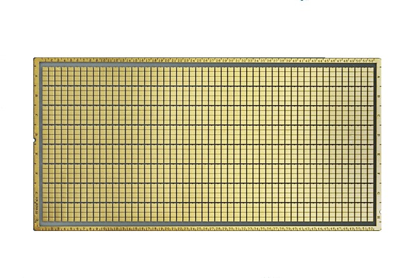
Types de placage de circuits imprimés et leurs avantages et inconvénients
1. Nickel doré par immersion sans électrolyse (ENIG)
Avantages:
- Grande planéité de la surface, idéale pour le brasage SMT à pas fin (par exemple, BGA), réduisant les défauts de brasage.
- La couche d'or offre une excellente stabilité chimique, empêchant l'oxydation et garantissant la fiabilité des contacts à long terme (par exemple, interfaces USB/PCIe).
- La couche de nickel agit comme une barrière de diffusion, améliorant la durabilité des joints de soudure.
Inconvénients:
- Processus complexe avec des coûts plus élevés.
- Risque de défaut du "black pad" (oxydation du nickel) à haute température/humidité, affectant la soudabilité.
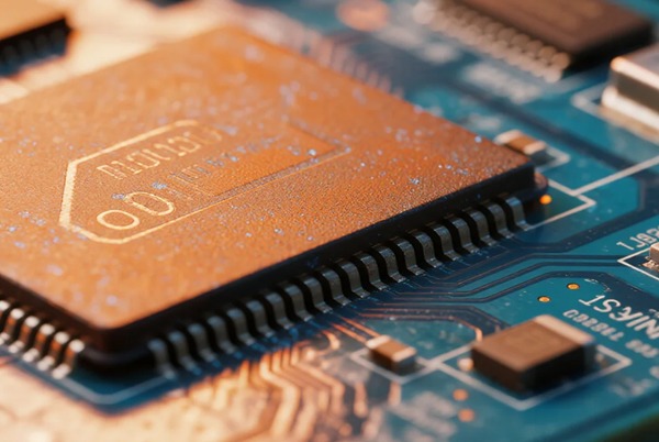
Applications: Domaines à haute fiabilité tels que les équipements de communication et les cartes mères de serveurs, en particulier pour les circuits imprimés à haute fréquence et à haute densité.
2.Placage étain/plomb (Sn/Pb)
Avantages:
- Excellente mouillabilité de la soudure et performances de soudage à basse température.
- Processus peu coûteux et mature.
Inconvénients:
- Le plomb est toxique et fait l'objet de restrictions dans le cadre de la directive RoHS et des réglementations environnementales.
- Ils ont tendance à se déformer à haute température, ce qui réduit leur résistance mécanique.
Applications: En voie de disparition ; utilisé uniquement dans certains produits électroniques grand public à bas prix (par exemple, les jouets bon marché).
Vous souhaitez choisir le procédé de galvanisation de circuits imprimés le mieux adapté à votre produit ? Consulter nos experts techniques pour obtenir des solutions personnalisées !
3.Conservateur de soudabilité organique (OSP)
Avantages:
- Processus simple et très peu coûteux.
- Compatible avec la soudure sans plomb, convient aux conceptions à haute densité.
Inconvénients:
- Couche mince, sujette à l'oxydation ; courte durée de conservation (généralement 6 mois).
- Ne résiste pas à de multiples cycles de refusion.
Applications: Électronique grand public (par exemple, smartphones, appareils électroménagers) et produits à rotation rapide.
4.Argent d'immersion
Avantages:
- Conductivité supérieure, idéale pour la transmission de signaux à haute fréquence.
- Coût inférieur à celui de l'ENIG ; bonne résistance aux hautes températures.
Inconvénients:
- Susceptible de ternir sous l'effet du soufre (nécessite un stockage scellé).
- Fenêtre de soudage étroite.
Applications: Modules de puissance, électronique automobile et circuits à haute fréquence.
5.Placage en or dur
Avantages:
- Grande résistance à l'usure, convient pour les enfichages fréquents (par exemple, les connecteurs de bord).
- Faible perte de signal dans les applications à haute fréquence.
Inconvénients:
- Une couche d'or épaisse entraîne un coût très élevé.
- Il peut affecter la précision de la soudure pour les composants à pas fin.
Applications: Aérospatiale, équipements militaires et connecteurs haute fréquence.
6.Nickel chimique Palladium chimique Or d'immersion (ENEPIG)
Avantages:
- Combine la fiabilité de l'ENIG avec une meilleure soudabilité.
- Couche d'or plus uniforme, réduction du risque de "black pad".
Inconvénients:
- Un contrôle strict du processus (sensibilité au pH/à la température) réduit le rendement.
- Coût plus élevé que celui de l'ENIG.
Applications: Serveurs haut de gamme, appareils médicaux et applications à très haute fiabilité.
7.Mise à niveau de la soudure à l'air chaud (HASL)
Avantages:
- Processus mature et peu coûteux.
- L'épaisse couche de soudure assure une bonne protection.
Inconvénients:
- Un revêtement inégal (HASL vertical) peut affecter la soudure.
- L'air chaud à haute température peut endommager les substrats minces.
Applications: Cartes de contrôle industrielles et électronique grand public bas de gamme (le procédé HASL horizontal est courant).
Problèmes courants et solutions dans le processus de galvanoplastie
1. Épaisseur de placage non uniforme
Symptômes:
- Épaisseur de placage inégale sur la surface du circuit imprimé, avec des zones localisées de surplacage, de sous-placage ou de saut.
Causes profondes:
- Problèmes d'électrolytes: Déséquilibre de concentration ou distribution inégale des ions.
- Distribution actuelle: Mauvais positionnement du circuit imprimé ou mauvaise conception de l'anode entraînant une densité de courant inégale.
- Agitation insuffisante: Une mauvaise circulation de l'électrolyte entraîne une diffusion inadéquate des ions.
Solutions:
- Optimisation des processusAjuster l'angle d'accrochage du circuit imprimé et optimiser la géométrie et la disposition de l'anode.
- Contrôle dynamique: Mettre en œuvre une agitation mécanique/par air et contrôler/réapprovisionner régulièrement l'électrolyte.
- Étalonnage des paramètres: Utiliser les tests de la cellule de Hull pour vérifier l'uniformité de la distribution du courant.
2.Mauvaise adhérence du placage
Symptômes:
- Décollement ou écaillage du placage en raison d'une faible liaison avec le substrat.
Causes profondes:
- Défauts de prétraitement: Huiles résiduelles, oxydes ou microgravure insuffisante sur la surface du cuivre.
- Problèmes liés aux bains de placage: Déséquilibre des additifs ou contamination organique.
- Écart de processus: Température/pH/temps en dehors de la plage spécifiée.
Solutions:
- Prétraitement amélioré: Ajouter des étapes de nettoyage chimique et de micro-gravure pour assurer l'activation de la surface.
- Gestion des bains: Analyse régulière de la composition, réapprovisionnement en additifs et filtration des impuretés.
- Normalisation des paramètres: Définir des fenêtres de processus et surveiller les paramètres clés (par exemple, température ±2°C, pH ±0,5).
3.Surface de placage rugueuse
Symptômes:
- Placage granuleux ou piqué avec un mauvais état de surface.
Causes profondes:
- Contamination: Particules métalliques ou poussières dans le bain de placage.
- Courant excessif: Cristallisation grossière conduisant à des dépôts poreux.
- Appauvrissement additif: Insuffisance d'azurants ou dégradation thermique.
Solutions:
- Entretien du bain: Installez une filtration continue (filtres de 1 à 5 µm) et remplacez périodiquement les sacs filtrants.
- Optimisation actuelle: Calculer la densité de courant appropriée (par exemple, 2-3 ASD) en fonction de l'épaisseur et de la surface de la carte.
- Contrôle des additifs: Réapprovisionner les azurants en temps voulu et éviter la dégradation à haute température.
4.Décoloration du placage
Symptômes:
- Noircissement de la dorure ou ternissement de l'argenture par immersion.
Causes profondes:
- Post-traitement incomplet: Solution de placage résiduelle ou eau de rinçage provoquant des réactions chimiques.
- Stockage insuffisant: Une humidité élevée ou une exposition au soufre/chlore accélère la corrosion.
- Contamination des bains: Impuretés excessives de métaux lourds (par exemple, Cu²⁺).
Solutions:
- Rinçage amélioré: Mettre en œuvre un rinçage à l'eau déminéralisée en trois étapes avec des additifs antioxydants.
- Contrôle du stockage: Maintenir un taux d'humidité ≤40% et utiliser un emballage résistant à l'humidité.
- Purification du bain: Le traitement au charbon actif ou l'électrolyse à faible courant permettent d'éliminer les impuretés.
5.Mauvaise soudabilité
Symptômes:
- Joints froids, pontage ou mauvais mouillage de la soudure.
Causes profondes:
- Contamination de la surface: Oxydes ou résidus organiques gênant l'étalement de la soudure.
- Défauts de placage: Variation d'épaisseur ou rugosité excessive.
- Écart de composition: Anomalies dans le rapport d'alliage (par exemple, teneur anormale en nickel phosphore).
Solutions:
- Mesures de protection: Terminer la soudure dans les 24 heures ou utiliser le scellement sous vide.
- Amélioration des processus: Adopter la métallisation par impulsion pour l'uniformité (Ra cible ≤0,2 µm).
- Essais de soudabilitéValider les performances du placage par des tests sur les billes de soudure.

Méthodes pour améliorer l'efficacité et la qualité de la métallisation des circuits imprimés
Optimisation des paramètres des équipements et des procédés
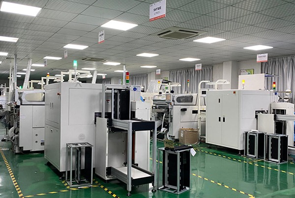
1.Maintenance et modernisation des équipements
- Système de maintenance préventive
- Établir des registres de maintenance pour les équipements clés (cuves de placage, agitateurs, systèmes de chauffage) avec des plans d'inspection quotidiens/hebdomadaires/mensuels.
- Utiliser des analyseurs de vibrations pour surveiller l'état des moteurs des mélangeurs et détecter à l'avance les défaillances potentielles (par exemple, l'usure des roulements).
- Réaliser une imagerie thermique infrarouge sur les redresseurs afin de prévenir les fluctuations de courant causées par un mauvais contact.
- Applications des équipements intelligents
- Introduction d'un équipement de galvanoplastie adaptatif doté de capteurs de concentration en temps réel pour l'ajustement automatique du bain
- Appliquer la technologie d'agitation par lévitation magnétique pour éliminer les zones mortes et améliorer l'uniformité du flux de la solution.
- Déployer des systèmes d'inspection par vision pour détecter automatiquement les défauts de placage et ajuster les paramètres du processus
2. Contrôle de processus de précision
- Gestion dynamique du courant
- Développer les modèles actuels de densité et de qualité du revêtement pour adapter automatiquement les paramètres en fonction de l'épaisseur de la carte et de la taille de l'ouverture
- Mise en œuvre d'une métallisation par impulsions (par exemple, impulsions à haute fréquence de 20 kHz) afin de réduire les effets de bord et d'améliorer l'uniformité.
- Utilisation d'une commande d'anode par zone pour un réglage indépendant de la distribution du courant
- Coordination température-temps
- Déployer des systèmes de contrôle multi-variables pour limiter les fluctuations de température à ±0,5°C
- Pour les procédés ENIG, établir des équations de taux de croissance du nickel pour calculer le temps de dépôt optimal.
- Installer des dispositifs d'auto-compensation du pH dans les cuves de métallisation pour maintenir la stabilité du processus.
Amélioration des processus de pré/post-traitement
1. Prétraitement avancé
- Solutions d'ultra-nettoyage
- Remplacer le nettoyage chimique par un traitement au plasma pour une propreté de niveau nanométrique (angle de contact <5°)
- Développer des formules composites de microgravure (par exemple, H₂SO₄-H₂O₂) pour contrôler la rugosité de la surface du cuivre (0,3-0,8μm).
- Intégrer des testeurs d'énergie de surface en ligne pour une évaluation quantitative du prétraitement
- Processus d'activation Innovations
- Utiliser des solutions d'activation catalysées par le palladium pour une couverture uniforme des parois des pores
- Appliquer la technologie d'activation sélective pour les cartes HDI afin d'éviter la surgravure dans les trous borgnes
2. Post-traitement complet
- Systèmes intelligents de nettoyage/séchage
- Conception d'un rinçage à contre-courant en trois étapes (40 % d'économies d'eau)
- Mettre en œuvre le séchage sous vide (<50ppm d'humidité résiduelle)
- Appliquer un rinçage de protection cathodique pour les couches d'or afin de prévenir les réactions de remplacement.
- Technologies de protection à long terme
- Développer des revêtements de monocouches auto-assemblées (SAM) pour prolonger l'anti-ternissement de l'argent jusqu'à 6 mois
- Intégrer des absorbeurs d'oxygène et des inhibiteurs de corrosion à la vapeur dans l'emballage
- Adoption du scellement des pores par laser pour les revêtements de panneaux à haute fréquence
Optimisation du système de gestion de la production
1. Surveillance intelligente de la qualité
- Réseau d'inspection en ligne
- Déploiement de la mesure d'épaisseur par EDXRF pour une inspection à 100 % du revêtement
- Développer des plateformes de vision IA pour identifier automatiquement 12 types de défauts de surface
- Appliquer l'analyse d'impédance pour évaluer la densité du revêtement
- Optimisation basée sur les données
- Établir des modèles de jumeaux numériques pour prédire les impacts des changements de paramètres
- Mettre en œuvre le contrôle SPC pour atteindre un CPK ≥1,67
- Permettre la traçabilité via les systèmes MES (jusqu'au niveau de la carte unique)
2. Développement des compétences du personnel
- Système de formation par paliers
- Basique : formation à la simulation VR (plus de 50 scénarios de défaillance)
- Avancé : Certification Six Sigma Green Belt
- Expert : Laboratoires de recherche sur la métallisation collaborant avec les universités
- Innovations en matière de gestion des performances
- Adopter un "système de points de qualité" en intégrant les améliorations de processus dans les indicateurs clés de performance.
- Lancer des prix de l'innovation avec participation aux bénéfices pour les brevets
- Mettre en œuvre une promotion à deux voies (voies parallèles gestion/technique)
Applications des technologies émergentes
- Développer le placage au CO₂ supercritique pour réduire de 90 % les eaux usées
- Essai de dépôt de couches atomiques (ALD) pour le contrôle de l'épaisseur au niveau nanométrique
- Recherche sur les revêtements composites renforcés au graphène pour améliorer de 300 % la résistance à l'usure
Vous êtes toujours confronté à des problèmes de galvanoplastie sur PCB ? Cliquez pour obtenir une évaluation gratuite du processuset notre équipe d'experts vous fournira une solution personnalisée !


Articles connexes