Qu'est-ce que le SMT dans l'assemblage de circuits imprimés ?
Table des matières
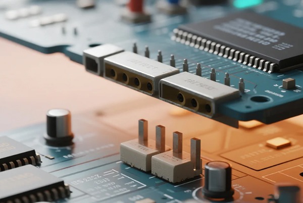
1. Présentation et définition de la technologie SMT
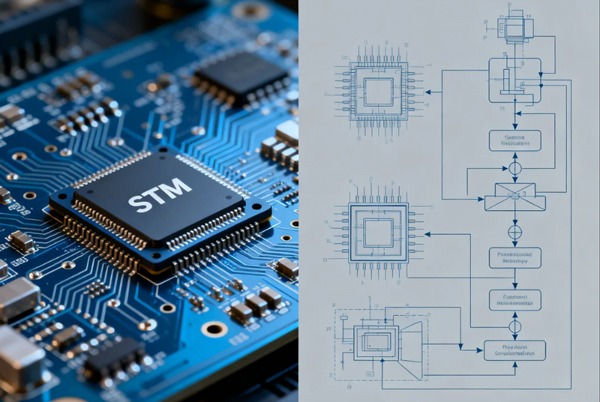
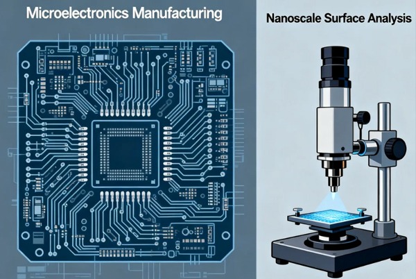
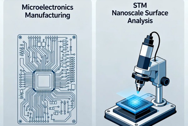
Technologie de montage en surface Le montage en surface (SMT) est la technologie et le procédé les plus courants dans l'industrie de l'assemblage électronique. Il s'agit du montage direct de composants à montage en surface (SMC/SMD, composants à puce) sans broches ou avec des broches courtes sur la surface de cartes de circuits imprimés (PCB) ou d'autres substrats, permettant d'obtenir une connexion des circuits grâce à des procédés de soudage par refusion ou par immersion.
2. Déroulement de base du processus SMT
2.1 Chaîne de processus complète
Impression de pâte à souder → Placement des composants → Soudage par refusion → Inspection optique AOI → Retouche → Séparation des panneaux2.2 Détails du processus central
Processus d'impression de la pâte à braser
- Fonction : Transférer la pâte à souder ou l'adhésif sur les pastilles du circuit imprimé en vue du soudage des composants.
- Équipement : imprimante à pochoir haute précision entièrement automatique
- Poste : Partie avant de la chaîne de production SMT
- Exigences techniques : précision d'impression ±0,05 mm, uniformité d'épaisseur >90 %.
Processus de placement des composants
- Fonction : Installation précise de composants montés en surface à des emplacements fixes sur un circuit imprimé.
- Équipement : machine multifonctionnelle de haute précision pour la prise et le placement
- Position : Processus après l'impression au pochoir
- Indicateurs techniques : précision de placement ±0,025 mm, vitesse >30 000 CPH
Procédé de soudage par refusion
- Fonction : le contrôle précis de la température fait fondre la pâte à souder afin d'obtenir une connexion fiable entre les composants et le circuit imprimé.
- Équipement : Four de refusion multizone
- Paramètres du processus :
- Zone de préchauffage : température ambiante → 150 °C, vitesse de chauffage 1-3 °C/seconde
- Zone de trempage : 150→180 °C, durée 60-120 secondes
- Zone de refusion : au-dessus de 183 °C, température maximale 210-230 °C
- Zone de refroidissement : vitesse de refroidissement 2-4 °C/seconde
AOI Inspection optique
- Fonction : Inspection automatisée de la qualité des soudures et de l'assemblage
- Capacités de détection : pièces manquantes, pièces incorrectes, mauvais alignement, polarité inversée, défauts de soudure, etc.
- Types d'équipements : AOI 2D/3D, systèmes d'inspection par rayons X
3. Types de processus SMT et applications
3.1 Processus d'assemblage simple face
Inspection à la réception → Impression de la pâte à souder → Placement des composants → Séchage → Soudage par refusion → Nettoyage → Inspection → RetoucheScénarios d'application: Produits électroniques grand public, modules de circuits simples
3.2 Processus d'assemblage double face
Solution A (Soudure par refusion complète) :
Côté A : Impression de pâte à souder → Placement des composants → Soudage par refusion
↓
Retournement du circuit imprimé
↓
Côté B : Impression de pâte à souder → Placement des composants → Soudage par refusion
↓
Nettoyage → Inspection → Retouche
Solution B (Soudure mixte) :
Côté A : Impression de pâte à souder → Placement des composants → Soudage par refusion
↓
Retournement du circuit imprimé
↓
Côté B : Distribution d'adhésif → Placement des composants → Durcissement → Soudage à la vague
↓
Nettoyage → Inspection → Retouche
3.3 Solutions mixtes pour les processus d'assemblage
SMD en premier, DIP en second (SMD > DIP) :
Inspection à la réception → Application d'adhésif côté B → Placement des composants → Durcissement
↓
Retournement → Insertion des composants côté A → Soudage à la vague
↓
Nettoyage → Inspection → Retouche
DIP en premier, SMD en second (DIP > SMD) :
Inspection à la réception → Insertion des composants côté A → Retournement
↓
Application d'adhésif côté B → Placement des composants → Durcissement
↓
Retournement → Soudage à la vague → Nettoyage → Inspection → Retouche
4. Analyse des avantages techniques du SMT
4.1 Avantages de la miniaturisation
- Taille des composants réduite à 1/10 de celle des composants DIP traditionnels
- Poids réduit de 60 à 80 %
- La densité d'assemblage a été multipliée par 3 à 5.
- Pas de plomb réduit à 0,3 mm
4.2 Amélioration des performances électriques
- L'inductance et la capacité parasites ont été réduites de plus de 50 %.
- Réduction de 30 % du délai de transmission des signaux
- Amélioration des caractéristiques haute fréquence, augmentation de la vitesse de fonctionnement
- La compatibilité électromagnétique (CEM) s'est considérablement améliorée.
4.3 Efficacité de la production et coûts
- Degré d'automatisation > 95 %
- L'efficacité de la production a été multipliée par 2 à 3.
- Réduction globale des coûts de 30 à 50 %
- Le taux d'utilisation des matériaux a augmenté de 40 %.
4.4 Qualité et fiabilité
- Taux de défauts des soudures < 50 ppm
- Résistance aux vibrations améliorée de 5 à 10 fois
- Taux de défaillance des produits réduit de 60 %
- Temps moyen entre pannes (MTBF) prolongé
5. Système de contrôle qualité
5.1 Combinaison des méthodes de détection
- Inspection en ligne: AOI, SPI (inspecteur de pâte à souder)
- Inspection hors ligne: Rayons X, test à sonde volante ICT
- Test fonctionnel: Testeur fonctionnel FCT
- Analyse microscopique: Microscope, microscope électronique
5.2 Points clés de contrôle des processus
- Contrôle de l'épaisseur d'impression de la pâte à souder : 0,1-0,15 mm
- Contrôle de la précision de positionnement : ±0,05 mm
- Surveillance en temps réel du profil de température de soudage par refusion
- Gestion des dispositifs sensibles à l'humidité (MSD)
6. Tendances en matière de développement technologique
6.1 Progrès en matière de miniaturisation
- Application de production en série de composants de taille 01005
- Technologie de micro-espacement à pas de 0,3 mm
- Intégration d'emballages empilés en 3D (SiP)
6.2 Fabrication intelligente
- Système d'exécution de la fabrication (MES)
- Contrôle qualité par vision industrielle et intelligence artificielle
- Optimisation du processus de jumelage numérique
- Systèmes de maintenance prédictive
6.3 Fabrication écologique
- Procédé de soudage sans plomb
- Produits nettoyants à faible teneur en COV
- Réduction de la consommation d'énergie de 30 %
- Taux de recyclage des déchets > 95 %
7. Expansion du champ d'application
- Electronique grand public: Smartphones, tablettes, appareils portables
- Équipement de communication: stations de base 5G, modules de communication optique
- Électronique automobile: Systèmes ADAS, divertissement embarqué
- Contrôle industriel: PLC, ordinateurs industriels
- Électronique médicale: Équipement de surveillance, instruments de diagnostic
- Aérospatiale: Communication par satellite, contrôle de vol
En tant que processus fondamental de la fabrication électronique moderne, la technologie SMT continue de favoriser la miniaturisation, l'amélioration des performances et la fiabilité accrue des produits électroniques grâce à une innovation technologique et une optimisation des processus continues, apportant ainsi un soutien important au progrès technologique de l'industrie de l'information électronique.


Articles connexes