Introduction:
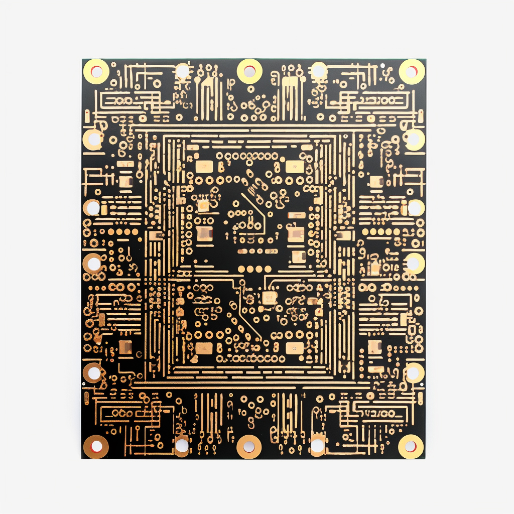
In the fast-paced world of electronics manufacturing, High-Density Interconnect (HDI) printed circuit boards (PCBs) have emerged as a game-changer. With their compact size, high circuit density, and enhanced performance, HDI PCBs are revolutionizing the industry. This article explores the benefits and applications of HDI PCB prototypes, highlighting their role in advancing electronics manufacturing.

What are HDI PCB prototypes?
HDI PCB prototypes are advanced circuit boards that utilize High-Density Interconnect technology. Unlike traditional PCBs, HDI PCBs feature intricate designs with multiple layers, microvias, and fine-pitch components. These prototypes serve as a testing ground for new product designs, allowing manufacturers to evaluate the functionality, performance, and manufacturability of their electronic devices.
The benefits of HDI PCB prototypes:
a. Miniaturization: HDI PCB prototypes enable the miniaturization of electronic devices. With their high circuit density and compact size, manufacturers can design smaller and lighter products without compromising functionality.
b. Enhanced Performance: HDI PCBs offer improved signal integrity, reduced noise, and better power distribution. The shorter interconnects and smaller vias minimize signal loss and crosstalk, resulting in higher-speed and more reliable electronic devices.
c. Design Flexibility: HDI PCB prototypes provide greater design flexibility, allowing manufacturers to incorporate complex features such as blind and buried vias, microvias, and fine-pitch components. This flexibility opens up new possibilities for innovative product designs.
d. Cost Optimization: While HDI PCB prototypes may have a higher initial cost compared to traditional PCBs, they can lead to cost savings in the long run. The compact size and reduced material usage result in lower production costs, improved energy efficiency, and reduced waste.
What’s the applications of HDI PCB prototypes:
HDI PCB prototypes find applications in various industries, including:
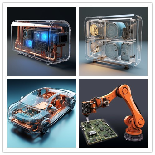
a. Consumer Electronics: HDI PCBs are widely used in smartphones, tablets, wearables, and other portable devices. Their compact size and high circuit density allow for sleek and lightweight designs without compromising performance.
b. Automotive: HDI PCB prototypes are crucial in automotive electronics, enabling advanced driver-assistance systems (ADAS), infotainment systems, and vehicle connectivity. The high-speed and reliable signal transmission of HDI PCBs ensure the seamless operation of these systems.
c. Medical Devices: HDI PCB prototypes play a vital role in medical devices, where space is often limited. They are used in devices such as pacemakers, implantable devices, and diagnostic equipment, ensuring precise and reliable performance.
d. Aerospace and Defense: HDI PCB prototypes are utilized in aerospace and defense applications, where reliability and performance are critical. They are used in avionics systems, satellites, radar systems, and communication equipment.

How to choose an HDI PCB prototype manufacturer:
When selecting an HDI PCB prototype manufacturer, consider the following factors:
a. Expertise: Look for a manufacturer with extensive experience in HDI PCB manufacturing and prototyping. They should have a deep understanding of the technology and be able to provide guidance throughout the prototyping process.
b. Advanced Manufacturing Capabilities: Ensure that the manufacturer has state-of-the-art equipment and technologies to produce high-quality HDI PCB prototypes. This includes capabilities such as laser drilling, microvia formation, and precise component placement.
c. Quality Control: Quality is paramount in HDI PCB prototypes. Choose a manufacturer that follows strict quality control processes and holds certifications such as ISO 9001. This ensures that the prototypes meet the highest standards of performance and reliability.
d. Collaboration and Support: Look for a manufacturer that offers collaborative support throughout the prototyping process. They should be responsive to your needs, provide design for manufacturing (DFM) feedback, and offer assistance in optimizing your design for manufacturability.
Conclusion:
HDI PCB prototypes are transforming the electronics manufacturing industry with their compact size, high circuit density, and enhanced performance. Topfast PCB is such a manufacturer with 20+ years experiences on HDI pcb prototype manufacturing and other types of PCBs such as: high speed PCBs, flexible PCBs, ceramic PCBs and metal PCBs... These prototypes enable manufacturers to push the boundaries of design, miniaturization, and functionality. By partnering with an experienced HDI PCB prototype manufacturer like Topfast PCB, you can unlock new possibilities for innovative electronic devices and stay ahead in the competitive market.
Address of Plant
PCB Factory:
A1 Building, B Zone, Ditang Industrial Zone, Ditang Road, Shajing Street, Bao'an District, Shenzhen, China
PCBA Factory:
4/F, Building 21, No. 46 Xinye Road, Yonghe Development Zone, Huangpu District, Guangzhou, China
Office Address:
Room 2201-03 & 2206, Building 1, Changfeng International, No. 96, Li Xin 12 Road, Zengcheng District, Guangzhou City, Guangdong Province, China.