Медное покрытие - это Критический шаг, превращающий просверленные отверстия в надежные электрические соединения.
Независимо от того, насколько хорошо разработана печатная плата, некачественное медное покрытие может привести к этому:
- Прерывистые соединения
- Через взлом
- Преждевременный отказ изделия
С точки зрения производителя, медное покрытие - это не просто химический процесс, это ворота надежности.
В этой статье рассказывается о том, как работает медное покрытие при производстве печатных плат, о различных этапах нанесения покрытия и о том, как производители, такие как 3. Топфаст контролируйте качество покрытия для обеспечения долговременной работы.
Ii. Содержание
Что такое медное покрытие в производстве печатных плат?
Медное покрытие - это процесс нанесение меди на поверхности печатных плат и внутри просверленных отверстий для создания электрических соединений между слоями.
Нанесение покрытия служит двум основным целям:
- Обеспечение непрерывности электрического тока через отверстия
- Достижение необходимой толщины меди для обеспечения тока и надежности
Виды медного покрытия при производстве печатных плат
Безэлектродное медное покрытие
Электролитическое медное покрытие осаждает тонкий, равномерный слой меди без использования электрического тока.
Назначение
- Создание начального проводящего слоя внутри просверленных отверстий
- Подготовьте печатную плату к нанесению гальванического покрытия
Обычная толщина:
- ~1-3 микрона
Этот шаг необходим для придания электрической функциональности отверстиям.
Электролитическое медное покрытие
Гальваническое покрытие использует электрический ток для наращивания толщины меди.
Назначение
- Укрепление стен
- Увеличение толщины поверхностной меди
- Соответствие проектным характеристикам меди
Гальваническое покрытие определяет:
- Через надежность
- Пропускная способность по току
- Механическая прочность

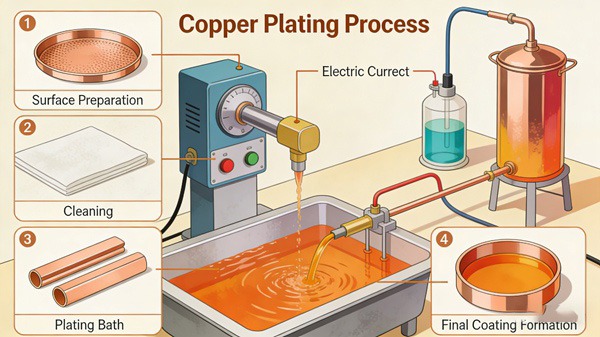
Пошаговый процесс нанесения медного покрытия
Шаг 1 - Подготовка стенки отверстия
После сверления необходимо обработать стенки отверстия:
- Очищенный
- Опустошенный
- Активирован для осаждения меди
Плохая подготовка приводит к слабой адгезии меди.
Шаг 2 - Осаждение меди электролитическим способом
Тонкий слой меди осаждается химическим способом, обеспечивая:
- Равномерное покрытие
- Непрерывность электропроводки
Этот слой является основой для всех последующих покрытий.
Шаг 3 - Наращивание толщины гальванического покрытия
Толщина меди увеличивается за счет контролируемого гальванического покрытия.
Ключевые параметры включают:
- Плотность тока
- Химия для ванн
- Температура
- Время нанесения покрытия
Последовательность здесь имеет решающее значение для надежности.
Толщина покрытия и почему она имеет значение
Толщина стенок
Надежность улицы в значительной степени зависит от:
- Минимальная толщина меди
- Равномерное распределение
Недостаточное количество меди может стать причиной:
- Трещины при термоциклировании
- Разомкнутые цепи
Поверхность Толщина меди
Поверхность поражена медью:
- Мощность трассирующего тока
- Производительность травления
- Контроль импеданса
В компании TOPFAST толщина покрытия тщательно подбирается в соответствии с требованиями проекта, чтобы избежать чрезмерного или недостаточного покрытия.
Распространенные дефекты медного покрытия
H3: Тонкое покрытие
Вызвано:
- Недостаточное время нанесения покрытия
- Плохое распределение тока
Это приводит к снижению надежности.
Формирование пустоты
Пустоты внутри отверстий могут возникать из-за:
- Плохая очистка отверстий
- Неполное электролитическое покрытие
Пустоты - это серьезный риск для надежности.
Неравномерное покрытие
Неравномерное распределение меди приводит к:
- Слабые стены
- Изменение импеданса
- Потеря урожая
Как медное покрытие влияет на надежность печатных плат
Качество медного покрытия оказывает непосредственное влияние:
- Характеристики термоциклирования
- Устойчивость к механическим нагрузкам
- Долговременная электрическая стабильность
В высоконадежных приложениях качество покрытия часто имеет большое значение больше, чем просто внешний вид доски.
Факторы дизайна, влияющие на качество покрытия
С точки зрения производства, нанесение покрытия становится более сложной задачей, когда:
- Соотношение сторон слишком велико
- Размер отверстия слишком мал
- Распределение меди неравномерно
- Используются тяжелые медные конструкции
Ранний анализ DFM помогает выявить риски нанесения покрытия до начала производства.
Перспективы производителя: как TOPFAST контролирует качество покрытия
В компании TOPFAST качество медного покрытия обеспечивается за счет:
- Контролируемое управление химическими ваннами
- Контроль толщины в режиме реального времени
- Регулярный анализ поперечного сечения
- Стандарты приемки, согласованные с IPC
- Обратная связь при проектировании на основе DFM
Основное внимание уделяется Стабильная урожайность и долгосрочная надежностьА не просто соответствовать минимальным требованиям.
Стоимость медных покрытий
Стоимость медного покрытия увеличивается по мере роста:
- Высокие требования к меди
- Проходы с высоким аспектным отношением
- Жесткие допуски по толщине
- Расширенные характеристики надежности
Оптимизация требований к гальваническому покрытию может значительно снизить стоимость печатной платы без ухудшения характеристик.
Iii. Выводы и рекомендации
Нанесение медного покрытия - один из самых ответственных процессов при производстве печатных плат.
Он превращает просверленные отверстия в прочные электрические соединения и определяет надежность печатной платы.
Понимая, как работает медное покрытие и что влияет на его качество, дизайнеры и покупатели могут принимать более разумные решения, которые уравновешивают стоимость, производительность и надежность.
Благодаря контролируемым процессам и производственному опыту, TOPFAST обеспечивает качество медного покрытия, которое поддерживает надежную работу печатной платы на протяжении всего жизненного цикла изделия.
Related Reading
Процесс производства печатных плат объясняется шаг за шагом
Изготовление внутреннего слоя: объяснение
Сверление печатных плат в сравнении с лазерным сверлением
Часто задаваемые вопросы о медном покрытии
О: Медное покрытие создает электрические соединения между слоями печатной платы и обеспечивает достаточную толщину меди для надежности.
О: Безэлектролитная гальваника создает начальный проводящий слой, а электролитическая гальваника наращивает толщину меди с помощью электрического тока.
О: Толщина медных витков зависит от конструкции и требований к надежности, но должна соответствовать стандартам IPC для долгосрочной работы.
О: Пустоты обычно возникают из-за плохой очистки отверстий или неполного покрытия электролизной медью.
О: Правильное медное покрытие повышает устойчивость к термическим нагрузкам, механической усталости и электрическим сбоям.