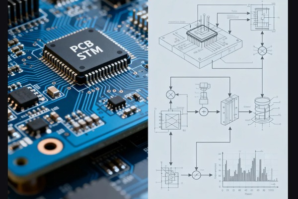
Каковы различные типы гальванического покрытия печатных плат?
Ii. Содержание
Типы покрытия печатных плат, их преимущества и недостатки
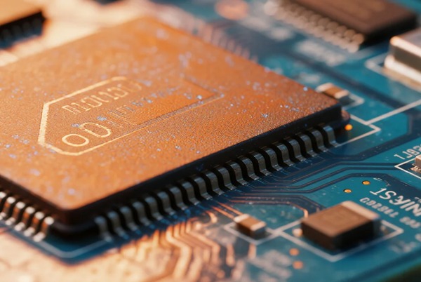
1. Золото с погружением в никель (ENIG)
Преимущества:
- Высокая плоскостность поверхности, идеально подходящая для SMT-пайки с мелким шагом (например, BGA), уменьшает дефекты пайки.
- Золотой слой обладает превосходной химической стабильностью, предотвращая окисление и обеспечивая долговременную надежность контактов (например, интерфейсы USB/PCIe).
- Слой никеля действует как диффузионный барьер, повышая прочность паяного соединения.
Недостатки:
- Сложный процесс с большими затратами.
- Риск возникновения дефекта “черная площадка” (окисление никеля) при высокой температуре/влажности, влияющего на паяемость.
Приложения: Высоконадежные области, такие как коммуникационное оборудование и материнские платы серверов, особенно для высокочастотных/высокоплотных печатных плат.
2.Оловянно-свинцовое покрытие (Sn/Pb)
Преимущества:
- Превосходная смачиваемость припоем и низкотемпературная пайка.
- Недорогой и отлаженный процесс.
Недостатки:
- Свинец является токсичным веществом, запрещенным RoHS и экологическими нормами.
- Склонны к ползучести при высоких температурах, что снижает механическую прочность.
Приложения: Снимается с производства; используется только в некоторой недорогой потребительской электронике (например, в дешевых игрушках).
Хотите выбрать наиболее подходящий процесс гальванизации печатных плат для вашего продукта? Проконсультируйтесь с нашими техническими специалистами прямо сейчас чтобы получить индивидуальные решения!
3. Органический консервант паяемости (OSP)
Преимущества:
- Простой процесс и очень низкая стоимость.
- Совместимы с бессвинцовой пайкой, подходят для конструкций высокой плотности.
Недостатки:
- Тонкое покрытие, склонное к окислению; короткий срок хранения (обычно <6 месяцев).
- Не устойчивы к многократным циклам дожигания.
Приложения: Потребительская электроника (например, смартфоны, бытовая техника) и быстро оборачиваемые продукты.
4.Погружное серебро
Преимущества:
- Превосходная проводимость, идеальная для передачи высокочастотных сигналов.
- Более низкая стоимость по сравнению с ENIG; хорошая устойчивость к высоким температурам.
Недостатки:
- Восприимчивы к потускнению под воздействием серы (требуют герметичного хранения).
- Узкое окно процесса пайки.
Приложения: Силовые модули, автомобильная электроника и высокочастотные цепи.
5.Твердое золотое покрытие
Преимущества:
- Высокая износостойкость, подходит для частых подключений (например, краевые разъемы).
- Низкие потери сигнала в высокочастотных приложениях.
Недостатки:
- Толстый слой золота приводит к очень высокой стоимости.
- Это может повлиять на точность пайки компонентов с мелким шагом.
Приложения: Аэрокосмическая промышленность, военное оборудование и высокочастотные разъемы.
6. Погружное золото без электролитического никеля и безэлектролитического палладия (ENEPIG)
Преимущества:
- Сочетает в себе надежность ENIG и лучшую паяемость.
- Более равномерный слой золота, сниженный риск “черной площадки”.
Недостатки:
- Строгий контроль процесса (чувствительность к pH/температуре) снижает выход продукции.
- Более высокая стоимость по сравнению с ENIG.
Приложения: Высокопроизводительные серверы, медицинские устройства и сверхнадежные приложения.
7.Выравнивание горячим воздушным припоем (HASL)
Преимущества:
- Отработанный процесс и низкая стоимость.
- Толстое покрытие из припоя обеспечивает хорошую защиту.
Недостатки:
- Неравномерное покрытие (вертикальный HASL) может повлиять на пайку.
- Высокотемпературный горячий воздух может повредить тонкие подложки.
Приложения: Промышленные платы управления и бытовая электроника низкого класса (горизонтальный HASL является основным направлением).
Общие проблемы и решения в процессе нанесения гальванических покрытий
1. Неравномерная толщина покрытия
Симптомы:
- Неравномерная толщина покрытия на поверхности печатной платы, с локальными пере-, недо- или пропущенными участками.
Коренные причины:
- Проблемы с электролитами: Дисбаланс концентрации или неравномерное распределение ионов.
- Текущее распределение: Плохое расположение печатной платы или конструкция анода, что приводит к неравномерной плотности тока.
- Недостаточное перемешивание: Плохой поток электролита приводит к недостаточной диффузии ионов.
Решения:
- Оптимизация процессаРегулировка угла подвеса печатной платы и оптимизация геометрии/разметки анода.
- Динамический контроль: Осуществляйте механическое/воздушное перемешивание и регулярно контролируйте/дополняйте электролит.
- Калибровка параметров: Для проверки равномерности распределения тока используйте испытания на корпусных элементах.
2.Плохая адгезия покрытия
Симптомы:
- Отслаивание или шелушение покрытия из-за слабого сцепления с подложкой.
Коренные причины:
- Дефекты предварительной обработки: Остатки масел, окислов или недостаточное микротравление на медной поверхности.
- Проблемы с ваннами для нанесения покрытия: Дисбаланс добавок или органическое загрязнение.
- Отклонение процесса: Температура/ pH/ время вне заданного диапазона.
Решения:
- Улучшенная предварительная обработка: Добавьте этапы химической очистки и микротравления для обеспечения активации поверхности.
- Управление ванной: Регулярный анализ состава, пополнение добавок и фильтрация примесей.
- Стандартизация параметров: Определите технологические окна и контролируйте ключевые параметры (например, температуру ±2°C, pH ±0,5).
3.Грубая поверхность покрытия
Симптомы:
- Зернистое или ямочное покрытие с плохой отделкой поверхности.
Коренные причины:
- Загрязнение: Металлические частицы или пыль в ванне для нанесения покрытия.
- Чрезмерный ток: Крупная кристаллизация, приводящая к образованию пористых отложений.
- Аддитивное истощение: Недостаточное количество отбеливателей или термическая деградация.
Решения:
- Уход за ванной: Установите непрерывную фильтрацию (фильтры 1-5 мкм) и периодически заменяйте фильтровальные мешки.
- Текущая оптимизация: Рассчитайте соответствующую плотность тока (например, 2-3 ASD), исходя из толщины/площади платы.
- Контроль добавок: Пополняйте запасы отбеливателей по графику и не допускайте их разрушения при высоких температурах.
4.Обесцвечивание покрытия
Симптомы:
- Почернение золотого покрытия или потускнение иммерсионного серебра.
Коренные причины:
- Неполное послелечебное лечение: Остатки гальванического раствора или промывочной воды, вызывающие химические реакции.
- Плохое хранение: Высокая влажность или воздействие серы/хлора ускоряют коррозию.
- Загрязнение ванны: Избыток примесей тяжелых металлов (например, Cu²⁺).
Решения:
- Улучшенное ополаскивание: Выполните 3-ступенчатую промывку водой DI с антиоксидантными добавками.
- Управление хранением: Поддерживайте влажность ≤40% и используйте влагонепроницаемую упаковку.
- Очищение ванны: Для удаления примесей используйте обработку активированным углем или слаботочный электролиз.
5.Плохая паяемость
Симптомы:
- Холодные соединения, мосты или плохое смачивание припоем.
Коренные причины:
- Загрязнение поверхности: Оксиды или органические остатки, препятствующие растеканию припоя.
- Дефекты покрытия: Изменение толщины или чрезмерная шероховатость.
- Отклонение в составе: Аномалии соотношения сплавов (например, аномальное содержание фосфора в никеле).
Решения:
- Защитные меры: Завершите пайку в течение 24 часов или используйте вакуумную герметизацию.
- Совершенствование процессов: Применяйте импульсное покрытие для обеспечения однородности (целевой Ra ≤0,2 мкм).
- Испытание на паяемостьПроверьте эффективность покрытия с помощью испытаний шариков припоя.
Методы повышения эффективности и качества покрытия печатных плат
Оптимизация оборудования и параметров процесса
1.Обслуживание и модернизация оборудования
- Система профилактического обслуживания
- Вести учет технического обслуживания основного оборудования (резервуары для гальванических покрытий, мешалки, системы отопления) с ежедневными, еженедельными и ежемесячными планами проверок
- Используйте виброанализаторы для контроля состояния двигателя миксера и заблаговременного обнаружения потенциальных неисправностей (например, износа подшипников).
- Проведите инфракрасное тепловизионное обследование выпрямителей, чтобы предотвратить колебания тока, вызванные плохим контактом
- Применение интеллектуального оборудования
- Представляем адаптивное гальваническое оборудование с датчиками концентрации в реальном времени для автоматической регулировки ванны
- Применение технологии магнитно-левитационного перемешивания для устранения мертвых зон и улучшения равномерности потока раствора
- Внедрение систем визуального контроля для автоматического обнаружения дефектов гальванического покрытия и настройки параметров процесса
2. Точное управление технологическим процессом
- Динамическое управление током
- Разработка текущих моделей качества плотности и покрытия для автоматического подбора параметров в зависимости от толщины платы/размера апертуры
- Применяйте импульсное покрытие (например, высокочастотные импульсы 20 кГц) для уменьшения краевых эффектов и улучшения однородности
- Использование зонального управления анодом для независимой регулировки распределения тока
- Координация температуры и времени
- Развертывание систем управления с несколькими параметрами для ограничения колебаний температуры в пределах ±0,5°C
- Для процессов ENIG необходимо составить уравнения скорости роста никеля для расчета оптимального времени осаждения
- Установите устройства автоматической компенсации pH в резервуарах для гальванических покрытий для поддержания стабильности процесса
Усовершенствованные процессы предварительной и последующей обработки
1. Усовершенствованная предварительная обработка
- Решения для ультрачистки
- Замените химическую очистку плазменной обработкой для обеспечения чистоты на наноуровне (угол контакта <5°)
- Разработка композитных формул микротравления (например, H₂SO₄-H₂O₂) для контроля шероховатости поверхности меди (0,3-0,8 мкм)
- Интеграция онлайновых тестеров поверхностной энергии для количественной оценки предварительной обработки
- Инновации в процессе активации
- Для равномерного покрытия стенок пор используйте растворы для активации, катализируемые палладием
- Применение технологии селективной активации для плат HDI для предотвращения перетравливания в глухих проходах
2. Комплексное постлечебное лечение
- Интеллектуальные системы очистки/сушки
- Разработать трехступенчатую противоточную промывку (экономия воды 40 %)
- Осуществить вакуумную сушку (остаточная влажность <50ppm)
- Применяйте катодную защитную промывку для золотых слоев для предотвращения реакций замещения
- Технологии долгосрочной защиты
- Разработка самособирающихся монослойных (SAM) покрытий, позволяющих продлить срок защиты серебра от потускнения до 6 месяцев
- Поглотители кислорода + ингибиторы паровой коррозии VCI в упаковке
- Использование лазерной герметизации пор для покрытий высокочастотных плат
Оптимизация системы управления производством
1. Интеллектуальный мониторинг качества
- Сеть онлайн-инспекций
- Развертывание системы измерения толщины EDXRF для 100% контроля покрытия
- Разработка платформ искусственного интеллекта для автоматического определения 12 типов дефектов поверхности
- Применяйте импедансный анализ для оценки плотности покрытия
- Оптимизация на основе данных
- Создание моделей цифрового двойника для прогнозирования воздействия изменения параметров
- Внедрить контроль SPC для достижения CPK ≥1,67
- Возможность отслеживания с помощью систем MES (вплоть до уровня отдельных плат)
2. Развитие компетенций рабочей силы
- Многоуровневая система обучения
- Базовый: обучение VR-симуляции (50+ сценариев неисправностей)
- Продвинутый: Сертификация "Зеленый пояс Six Sigma
- Эксперт: Исследовательские лаборатории по нанесению покрытий, сотрудничающие с университетами
- Инновации в области управления эффективностью
- Принять “Систему баллов качества”, интегрировав улучшения процесса в KPI.
- Учредить премии за инновации с распределением прибыли за патенты
- Внедрить двухступенчатое продвижение по службе (параллельное продвижение по управленческой и технической лестницам)
Новые технологические приложения
- Разработка сверхкритического CO₂ для нанесения покрытия, позволяющего сократить объем сточных вод на 90%
- Пробное атомно-слоевое осаждение (ALD) для контроля толщины на нанометровом уровне
- Исследование композитных покрытий, усиленных графеном, для повышения износостойкости на 300%
Все еще боретесь с проблемами гальванического покрытия печатных плат? Нажмите, чтобы получить бесплатную оценку процессаИ наша команда экспертов предложит вам индивидуальное решение!


Похожие посты