Flerskikts-PCB-teknik
Som PCB-kretskort Utvecklingen mot högfrekventa, höglagrade och multifunktionella applikationer gör att användningen av flerlagerkort blir alltmer utbredd och omfattar branscher som mobiltelefoner, fordonselektronik, bärbara enheter, servrar, datacenter, autonom körning och flyg- och rymdindustrin. Jämfört med enkelsidiga och dubbelsidiga kort kräver flerskiktskort ytterligare processer som laminering och routing av innerskikt, vilket resulterar i mer komplexa tillverkningsflöden och högre tekniska krav.
Innehållsförteckning
Kärnan i flerskiktskretskort
Jämfört med begränsningarna hos kretskort med ett eller två lager uppnår flerlagerskretskort mindre storlekar och högre prestanda genom att stapla ledande lager (signallager/kraftlager/jordlager), vilket uppfyller behoven hos moderna elektroniska enheter (t.ex. 5G och AI-hårdvara).
Ladda upp din design gratis DFM-analys + kostnadsoptimering
6 Stora fördelar med Kretskort med flera lager
- Ultrahög densitet: 50%+ storleksminskning, perfekt för wearables.
- Låg EMI-strålning: Plana ytor minskar störningarna (15 dB lägre än dubbelskiktskort).
- Förbättrad termisk hanteringVärmeavledningsbanor i flera lager förhindrar överhettning.
- Lättvikt: Färre kontakter minskar den totala vikten.
- Flexibel design (Tillval): Böjbar för speciella tillämpningar.
- Kostnadseffektivt: Lägre enhetskostnad vid massproduktion.
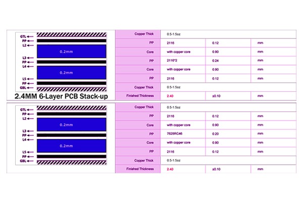
Stack-up design
| Skikt | Rekommenderad uppställning | Tillämpningar |
|---|---|---|
| 4L | Signal-Ground-Power-Signal | Konsumentelektronik (t.ex. smarta hem) |
| 6L | Signal-Ground-Signal-Signal-Signal-Power-Signal | Höghastighetskommunikation (DDR3/DDR4) |
| 8L+ | Symmetrisk stack-up + avskärmning | Militär/medicinsk utrustning med hög tillförlitlighet |
Arbetsflöde för tillverkning
- Teknisk granskning: Validering av Gerber-filer, DFM-analys.
- Bearbetning av inre lager: Kopparetsning + AOI-inspektion.
- LamineringLimning vid hög temperatur och högt tryck.
- Borrning & Plätering: Laserborrning + kemisk deponering av koppar.
- TestningImpedansprovning, inspektion med flygande sond.
Behov lågkostnadslösningar för flerskiktskretskort? Få en omedelbar offert
20+ tekniker för kostnadsoptimering för flerskikts-kretskort
1. Designoptimering (grundläggande kostnadsbesparande strategier)
✅ Minska antalet lager
- Prioritera 4/6-lagerskonstruktioner framför 8+ lager – varje minskning med två lager sänker kostnaderna med 15-25%.
- Användning Routning med hög densitet (t.ex. 3/3 mil spår/utrymme) för att minimera antalet lager.
✅ Regel för jämna lager
- Konstruktioner med udda lager kräver extra balanseringsmaterial, vilket ökar kostnaderna med 5-10%.
✅ Standardisera via design
- Använd genomgående hål ≥0,2 mm (undvik laserborrning, vilket ökar 30% kostnad).
- Eliminera blinda/begravda vior (HDI-processer) dubbla kostnader).
✅ Förenkla impedansregleringen
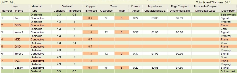
- Standardisera kritisk signalimpedans (t.ex. alla 50 Ω) för att minska antalet specialskikt.
✅ Optimera panelutnyttjandet
- Designa efter standardpanelstorlekar (t.ex. 18″×24″) för att minimera materialspill.
2.Materialval (spara 20-50%)
🔹 Val av substrat
- Användning FR-4 för konsumentelektronik (40% billigare än högfrekventa material).
- För höghastighetssignaler bör du överväga medel-Tg-material (t.ex. S1000-2) för balans mellan kostnad och prestanda.
🔹 Koppar Vikt
- Användning 1 oz inre lager (15% billigare än 2 oz), med selektiv förtjockning av det yttre lagret.
🔹 Ytfinish
- Föredrar HASL (60% billigare än ENIG); använd nedsänkt silver för högfrekventa behov.
3.Strategier för serieproduktion
📊 Volymrabatter
- Beställning 500+ enheter för 20% rabatt; 1.000+ enheter för en extra kostnad 5% rabatt.
📊 Delning av panel
- Kombinera små beställningar med andra kunder (förlänger ledtiden med 3-5 dagar men sänker kostnaderna med 30%).
4.Optimering av leveranskedjan
🛒 Lokaliserad sourcing
- Användning Shengyi Tech i stället för Rogers (sparar 70% på substrat).
- Källa komponenter från LCSC/LCSC Mall för kostnadseffektiva alternativ.
🛒 Beställningar under lågsäsong
- Lägg order i Q1/Q3 för 5% rabatt (undvik högsäsonger för konsumentelektronik).
5.DFM (Design for Manufacturability) Optimering
⚙️ Slappna av toleranser
- Tillåt ±10 % tolerans för spårbredd (sparar 8 % jämfört med ±5 %).
- Säkerställa lödmaskbroar ≥0,1 mm för att undvika dyra LDI-processer.
⚙️ Undvik specialprocesser
- Hoppa över guldfingrar (+20% kostnad), tung koppar (>3oz) och andra premiumfunktioner.
6.Provning och certifiering
📉 Provtagning över 100% inspektion
- Användning testning av flygande sond för prototyper (50% billigare än AOI).
- Välja IPC klass 2 i stället för klass 3 (sparar 25% för industriella tillämpningar).
7.Logistik & Leverans
🚚 Välj markfrakt
- För beställningar >100 kg, använd sjöfrakt (80% billigare än flyg, +7 dagars leveranstid).
Kostnadsbesparande jämförelsetabell
| Optimeringsmetod | Besparingar | Bäst för |
|---|---|---|
| 6 lager → 4 lager | 15-25% | Lågfrekvent elektronik |
| FR-4 vs. högfrekvent | 40-70% | Icke-mm-vågsapplikationer |
| Eliminera blinda vior | 30% | Icke-bärbara/tunna enheter |
| Lokaliserade substrat | 50%+ | Industriella styrkort |
| MOQ för 500 enheter | 20% | Prototyper för små och medelstora företag |
Fallstudier inom industrin
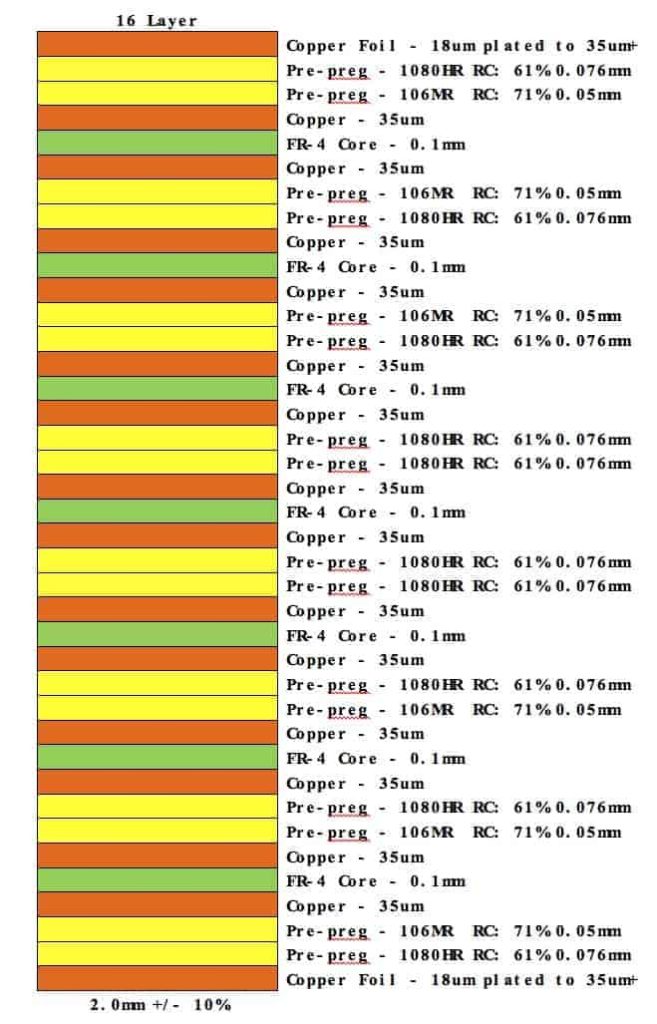
- Medicintekniska produkter: 16L kretskort för MRI-styrkort (±5 % impedansnoggrannhet).
- Elektronik för fordonsindustrin: 8L styv-flex PCB för vibrationsbeständighet.


Relaterade inlägg