Kretskort (PCB) är grunden för moderna elektroniska produkter. Även om många ingenjörer fokuserar på PCB-design är det färre som fullt ut förstår hur ett mönsterkort faktiskt tillverkas.
Att förstå tillverkningsprocessen för mönsterkort är till hjälp:
- Förbättra design för tillverkningsbarhet (DFM)
- Minska produktionskostnaden
- Undvik kvalitetsproblem
- Kommunicera mer effektivt med mönsterkortstillverkare
Denna artikel ger en tydlig, steg-för-steg-förklaring av PCB-tillverkningsprocessensom baseras på verkliga produktionsmetoder som används av TOPFAST, en professionell PCB-tillverkare som stöder prototyp- och massproduktion.
Innehållsförteckning
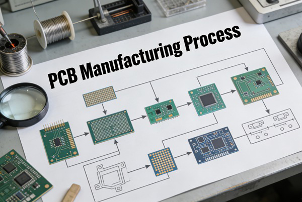
Översikt över tillverkningsprocessen för mönsterkort
Även om kretskortens komplexitet kan variera följer de flesta styva kretskort samma grundläggande tillverkningsflöde:
- Tillverkning av inre skikt
- Skiktuppriktning och laminering
- Borrning
- Kopparplätering
- Bildbehandling och etsning av yttre skikt
- Applicering av lödmask
- Ytfinish
- Silkscreentryck
- Elektrisk provning och slutbesiktning
Varje steg påverkar direkt kvalitet, avkastning och kostnad.
Steg 1 - Tillverkning av innerskikt
Bildbehandling av inre lager
Tillverkningen inleds med kopparpläterade laminatplåtar. Det önskade kretsmönstret överförs till kopparytan med hjälp av en fotoresist och UV-exponering.
Viktiga faktorer:
- Spårbredd och avståndsnoggrannhet
- Precision vid justering av foton
- Renrumsmiljö
Etsning av inre skikt
Oönskad koppar etsas bort på kemisk väg och kvar blir de nödvändiga kretsspåren.
Ur ett tillverkningsperspektiv:
- Finare spår ökar svårigheten att etsa
- Överetsning eller underetsning påverkar avkastningen
Hos TOPFAST optimeras parametrarna för etsning av det inre skiktet för att balansera precision och produktionsstabilitet.
Steg 2 - Skiktuppriktning och laminering
För flerskiktskretskort staplas de inre skikten med prepreg och yttre kopparfolier.
Lamineringsprocess
- Värme och tryck binder samman alla lager
- Exakt justering säkerställer korrekta via-anslutningar
Kostnads- och kvalitetspåverkan:
- Fler lager ökar lamineringscyklerna
- Sekventiell laminering ökar komplexiteten och kostnaderna
Steg 3 - Borrning
Borrning skapar hål för vior och komponentledningar.
Mekanisk borrning
Används för:
- Vior genomgående hål
- Större hålstorlekar
Borrningskostnaden ökar med:
- Mindre håldiametrar
- Högre bildförhållande
- Högt antal borrningar
Laserborrning (avancerade mönsterkort)
Laserborrning används för:
- Mikrovias i HDI-kretskort
Denna process kräver specialiserad utrustning och ökar tillverkningskostnaden.
Steg 4 - Kopparplätering
Efter borrning måste hålen vara elektriskt ledande.
Elektrolös kopparbeläggning
Ett tunt kopparskikt deponeras inuti de borrade hålen för att möjliggöra en elektrisk anslutning mellan skikten.
Elektroplätering
Ytterligare koppar är pläterad till:
- Förstärka vias
- Uppnå önskad koppartjocklek
Pläteringens jämnhet påverkar direkt tillförlitligheten, särskilt i applikationer med hög strömstyrka eller hög tillförlitlighet.
Steg 5 - Bildbehandling och etsning av det yttre skiktet
Det yttre lagrets kretsmönster formas med en process som liknar de inre lagrens.
Viktiga utmaningar:
- Bibehållen spårnoggrannhet efter plätering
- Kontroll av koppartjocklek
- Förhindrar kortslutning eller öppning
Bearbetningen av det yttre lagret har stor inverkan på slutlig avkastning.
Steg 6 - Applicering av lödmask
Syftet med lödmasken
Lödmask:
- Skyddar kopparspår
- Förhindrar lödning av bryggor
- Förbättrar elektrisk isolering
Vanliga färger är grönt, svart, blått och rött. Grönt är fortfarande det mest kostnadseffektiva och mest använda alternativet.
Kvalitetsfaktorer för lödmask
- Registreringens riktighet
- Maskens tjocklek
- Inledande definition
Dålig kvalitet på lödmasken kan orsaka monteringsfel senare.
Steg 7 - Ytbehandling
Ytfinishen skyddar exponerade kopparplattor och säkerställer lödbarheten.
Vanliga ytbehandlingsalternativ
- HASL: Kostnadseffektivt, används i stor utsträckning
- ENIG: Plan yta, högre tillförlitlighet
- OSP: Låg kostnad, begränsad hållbarhet
TOPFAST rekommenderar ytbehandlingar baserat på tillämpningskrav snarare än standardpreferenser.
Steg 8 - Silkscreentryck
Silkscreen tillägger:
- Referensbeteckningar för komponenter
- Polaritetsmarkeringar
- Logotyper eller identifierare
Även om den inte är elektriskt funktionell, förbättrar en klar silkscreen monteringsnoggrannheten och underhållet.
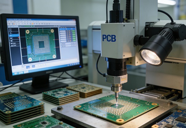
Steg 9 - Elektrisk testning och slutbesiktning
Elektrisk provning
Elektrisk provning verifierar:
- Kontinuitet
- Isolering
- Avsaknad av shorts och öppen
Detta steg är viktigt för att säkerställa funktionssäkerheten.
Slutlig kvalitetsinspektion
Slutbesiktning kan omfatta:
- Visuell inspektion
- AOI (automatiserad optisk inspektion)
- Dimensionella kontroller
På TOPFAST är inspektionsstandarderna anpassade till IPC-krav och kundspecifikationer.
Hur tillverkningsprocessen för mönsterkort påverkar kostnad och kvalitet
Varje tillverkningssteg introduceras:
- Processvariabilitet
- Överväganden om avkastning
- Kostnadskonsekvenser
Vanliga kostnadsdrivare inkluderar:
- Högt antal lager
- Små borrstorlekar
- Snäva toleranser
- Avancerade ytbehandlingar
Genom att förstå hela processen kan konstruktörerna optimera mönsterkortskonstruktioner för både kostnad och tillverkningsbarhet.
Tillverkarens perspektiv: Hur TOPFAST optimerar mönsterkortstillverkningen
Som PCB-tillverkare fokuserar TOPFAST på:
- Standardisering av processer
- Tidig DFM-återkoppling
- Avkastningsdrivet beslutsfattande
- Stabil och skalbar produktion
I stället för att driva på onödiga avancerade processer betonar TOPFAST tillverkningsvänliga konstruktioner som ger jämn kvalitet.
Slutsats
Tillverkningsprocessen för mönsterkort är en noggrant kontrollerad sekvens av steg som vart och ett bidrar till det slutliga kortets prestanda, tillförlitlighet och kostnad.
Genom att förstå hur mönsterkort tillverkas - från tillverkning av inre lager till slutkontroll - kan ingenjörer och inköpare fatta bättre design- och inköpsbeslut.
Med tillverkning i första hand, TOPFAST hjälper kunderna att förvandla komplexa konstruktioner till tillförlitliga och kostnadseffektiva mönsterkort.
FAQ om tillverkningsprocessen för PCB steg för steg
A: Standard PCB-tillverkning tar vanligtvis 5-10 arbetsdagar, beroende på komplexitet och kvantitet.
S: Varje steg är viktigt, men borrning och plätering är avgörande för den elektriska tillförlitligheten.
S: Ja, det stämmer. Flerskiktskretskort kräver ytterligare laminerings- och inriktningssteg.
S: Ja, det stämmer. Konstruktioner som är anpassade till tillverkningskapaciteten ger bättre utbyte och lägre kostnader.
S: TOPFAST använder standardiserade processer, DFM-granskning och omfattande inspektion för att säkerställa jämn kvalitet.