Geleneksel delik içi montajdan yüksek yoğunluklu ara bağlantılara teknolojik geçiş, yapay zekanın patlayıcı büyümesiyle birleştiğinde, PCB endüstrisinin teknolojik yörüngesini, ürün yapısını ve değer dağılımını temelden yeniden şekillendiriyor.
İçindekiler
PCB'ler için Yapay Zeka Hesaplama Donanımının Teknolojik Gereksinimlerinin Yükseltilmesi
Yüksek Katman Sayısı ve Yüksek Yoğunluklu Ara Bağlantılara Talep
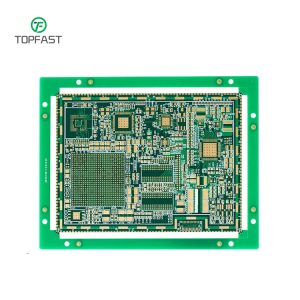
Geleneksel sunucu anakartları tipik olarak 12-16 katman kullanırken, mevcut ana akım yapay zeka eğitim sunucuları (NVIDIA DGX H100 serisi gibi) 20-30 katmanlı PCB katman sayıları gerektirmektedir. Özellikle GPU alt tabakaları için, 5.000 BGA lehim noktasını aşan ara bağlantı yoğunlukları gereklidir ve iz genişliği/aralığı geleneksel 4/4 milden 2/2 mil hatta 1,5/1,5 mile kadar sıkıştırılmıştır. Geleneksel eksiltici süreçler artık hassasiyet gereksinimlerini karşılayamadığından, bu tasarım talebi doğrudan mSAP'nin (Modifiye Yarı Eklemeli Süreç) benimsenmesine neden olmaktadır.
Sinyal Bütünlüğü Zorlukları ve Çözümleri
112 Gbps PAM4 iletim hızlarında, ekleme kaybı -0,6 dB/inç içinde kontrol edilmelidir. Simülasyon analizi yoluyla, dağılma faktörünün (Df) geleneksel FR-4 için 0,02'den 0,005'in altına düşürülmesi gerektiğini bulduk. Mevcut lider endüstri çözümü, 3,5±0,05'lik sabit bir Dk değerini koruyan ve 77 GHz'de bile iyi dielektrik özellikler sergileyen bir hidrokarbon reçine / seramik dolgu kompozit sistemi (Rogers RO4835™ gibi) kullanmayı içerir.
Termal Yönetim Teknolojisinde Yenilikler
Örnek olarak NVIDIA H100'ü ele alırsak, tek çipli tepe güç tüketimi 700W'a ulaşarak geleneksel termal tasarım çözümlerini tamamen yetersiz hale getirmektedir. Geliştirdiğimiz gömülü bakır blok + termal via dizisi teknolojisi termal direnci 0,8°C/W'a kadar düşürebilmektedir. Alt tabaka malzemesi seçimi açısından, yüksek Tg (≥170°C) ve yüksek termal iletkenlik (≥0,8 W/m-K) temel gereksinimler haline gelmiştir ve bazı üst düzey uygulamalar halihazırda metal alt tabakalar ve organik malzemelerden oluşan hibrit yapıları benimsemektedir.
Teknolojik Atılımlar ve Kilit Malzemelerin Yerelleştirilmesinde İlerleme
Gelişmeler Yüksek Frekans ve Yüksek Hızlı Bakır Kaplı Laminatlar
Shengyi Technology'nin S7439 serisi, uluslararası lider standartlara yaklaşarak 10 GHz'de 0,0058 Df değerine ulaşarak büyük OEM'ler tarafından onaylanmıştır. Sinoma Science & Technology'nin Düşük Dk elektronik cam kumaşı (Dk=4.2) geliştirmesi, Nittobo'nun teknolojik tekelini kırıyor ve 2025 yılına kadar seri üretim bekleniyor.
Özel Kimyasal Malzemeler
Lehim direnç mürekkeplerinde Taiyo Ink'in SR-7200G serisi, 20 μm'ye kadar çözünürlüklerle lazerle doğrudan görüntülemeyi destekler. Kaplama katkıları için MacDermid Enthone'un Circuposit 8800 serisi, 1:1 en-boy oranlarıyla tek tip kaplama sağlayarak yüksek katman sayılı PCB'ler için geçiş deliklerinde tek tip bakır kaplama sorununu ele alıyor.
Üretim Süreçlerindeki Teknik Darboğazlar ve Atılımlar
Lazer Delme Teknolojisi
CO2 lazerler, 0,1 mm'nin altında mikrovia işleme için fiziksel sınırlara yaklaşıyor. İşleme hassasiyetini 35 μm'ye çıkarmak için ışın şekillendirme teknolojisiyle birleştirilmiş UV lazer işleme sistemlerini tanıttık. Han's Laser'in 355 nm dalga boyu kullanan UV lazer delme makineleri, ±15 μm konumsal hassasiyetle minimum 50 μm delik çapı elde etmektedir.
Laminasyon Süreçlerinde Yenilikler
30'u aşan ultra yüksek katmanlı levhalar için, bölümlere ayrılmış ısıtma ve basınç uygulamasını içeren bir laminasyon işlemi geliştirdik. Reçine akışını hassas bir şekilde kontrol ederek, katmanlar arası dolum oranı 95%'nin üzerine çıkarılırken, katmanlar arası hizalama doğruluğu ±25 μm içinde tutulur.
Denetim Teknolojisindeki Gelişmeler
Birleştiren kapsamlı bir çözüm Otomatik Optik Muayene (AOI) ve elektriksel testler benimsenmiştir. Keysight'ın PathWave ADS yazılımı, 3D elektromanyetik alan simülasyonunu destekleyerek sinyal bütünlüğü sorunlarının erken tespit edilmesini sağlar. Devre içi testler için Teradyne'nin TestStation mimarisi, 112 Gbps arayüzler için bit hata oranı testini destekler.
Endüstriyel Zincirin Yeniden Yapılandırılması ve İş Modeli Dönüşümü
Tedarik Zinciri İlişkilerinin Yeniden Şekillenmesi
Yapay zeka sunucu PCB tedarik zinciri üç kademeye ayrılmıştır: GPU kart setleri çip üreticileri tarafından yönetilir (örneğin, NVIDIA'nın belirlenmiş tedarik zinciri); CPU anakartları geleneksel sunucu tedarik zincirini takip eder; ve modül üreticileri aksesuar modüllerini bağımsız olarak tedarik eder. Bu farklılaşma, PCB üreticilerinin farklılaştırılmış müşteri katılım yeteneklerine sahip olmasını gerektirmektedir.
Daha Yüksek Teknik Engeller Nedeniyle Artan Yoğunlaşma
18 katmanlı veya daha fazla PCB için sermaye yatırımı, geleneksel ürünlerin 3-5 katıdır ve Ar-Ge döngüleri 12-18 aya kadar uzanmaktadır. Bu durum, önde gelen şirketler arasında pazar payı yoğunlaşmasına yol açmış ve ilk üç üretici 2024 yılında yerel AI sunucu PCB pazarının 60%'sinden fazlasını oluşturmuştur.
Değer Dağılımındaki Değişimler
Yapay zeka sunucularının Malzeme Listesi (BOM) maliyetinde, PCB'lerin oranı geleneksel sunuculardaki 2-3%'den 6-8%'ye yükselmiştir. Özellikle GPU alt tabakaları için, yüksek teknik karmaşıklıkları nedeniyle, brüt marjlar geleneksel ürünler için 15-20%'den önemli ölçüde daha yüksek olan 35-40%'ye ulaşabilir.
Gelecekteki Teknolojik Gelişim Trendleri
Gelişmiş Ambalaj ve PCB'lerin Entegrasyonu
Chiplet mimarisi, PCB'lerin bazı interposer işlevlerini üstlenmesini gerektirmekte ve Substrat Benzeri PCB (SLP) teknolojisini 10/10 μm iz genişliğine/aralığına doğru yönlendirmektedir. Shennan Circuits'in geliştirdiği eSLP teknolojisi 8/8 μm işlem kapasitesine ulaşmıştır ve büyük çip üreticileri ile örnek doğrulama aşamasındadır.
Silikon Fotonik Birlikte Paketleme Teknolojisi
1,6T'nin üzerindeki optik modüller için Birlikte Paketlenmiş Optik (CPO) kaçınılmaz bir seçenek haline gelmiştir. Bu, PCB'lerin fotonik dalga kılavuzlarını entegre etmesini gerektirir ve 2026 yılına kadar mühendislik uygulamalarına ulaşması beklenen silikon dioksit dalga kılavuzlarına dayalı hibrit substrat teknolojisi geliştiriyoruz.
Sürdürülebilirlik Gereklilikleri
AB'nin CE-RED direktifi, PCB'lere halojensiz malzemeler ve kurşunsuz süreçler de dahil olmak üzere yeni çevresel gereklilikler getirmektedir. Geliştirdiğimiz biyo-bazlı epoksi reçine sistemimiz karbon ayak izini 40% oranında azaltmaktadır ve UL sertifikası almıştır.
Teknik Ekipler için Öneriler
Yetenek Yapısının Dönüşümü
Geleneksel süreç mühendislerinden "malzeme-süreç-sistem" kompozit yeteneklerine geçiş gereklidir. Ekibimizde malzeme bilimi geçmişine sahip mühendislerin oranı on yıl önce 10% iken bugün 35%'ye yükselmiştir.
Ar-Ge Yatırımlarının Odağı
Ar-Ge kaynaklarının 60%'sinin yüksek katman sayılı HDI'ye, 30%'sinin gelişmiş paketlemeye ve 10%'sinin sürdürülebilir geliştirme teknolojilerine ayrılması tavsiye edilmektedir. Çip üreticileri ile erken işbirliğine ve ön uç tasarımına katılıma özel önem verilmelidir.
Patent Yerleşim Stratejisi
Üç yönde patent düzenlerine odaklanın: yüksek hızlı malzemeler, termal dağılım yapıları ve yüksek yoğunluklu ara bağlantılar. Son yıllarda başvurulan temel patentlerimiz arasında, özel termal dağılım yapılarını içerenler 40%'yi oluşturmaktadır ve bu patentler gelecekte teknolojik bir bariyer haline gelecektir
Yapay zeka, PCB'leri yardımcı bileşenlerden bilgi işlem sistemlerinin temel parçalarına yükseltiyor. Durumdaki bu değişiklik, ürün geliştirme süreçlerini sistem düzeyinde bir zihniyetle yeniden tanımlamamızı ve saf üretim hizmeti sağlayıcılarından teknik çözüm sağlayıcılarına geçmemizi gerektiriyor. Gelecekteki endüstri rekabeti, malzeme sistemleri, süreç yetenekleri ve sistem tasarım becerilerinin kapsamlı bir yarışması olacaktır.