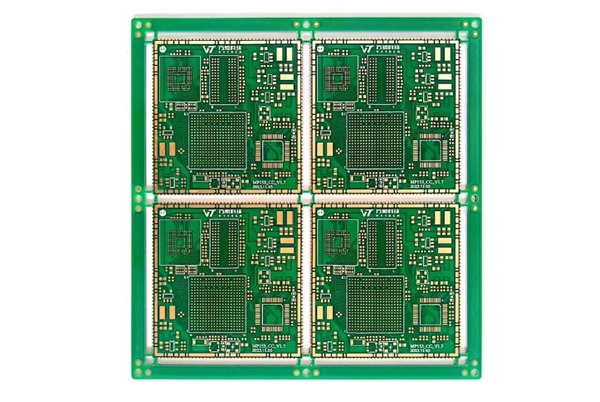
Der heutige Trend zu Miniaturisierung und hoher Leistung bei elektronischen Produkten ist ungebrochen, High-Density-Verbindung (HDI)-Leiterplatten sind zum zentralen Träger für elektronische Geräte der Spitzenklasse geworden. Ihre außergewöhnliche Leistung beruht auf äußerst präzisen Herstellungsverfahren und strengen Prüfstandards, um die Qualität und Zuverlässigkeit von HDI-Platten zu gewährleisten.
Inhaltsübersicht
HDI-Verständnis
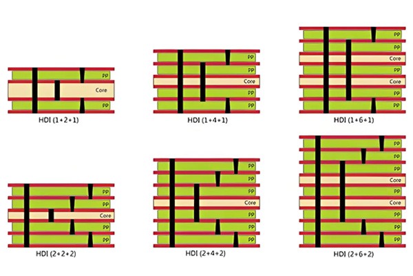
Bevor wir uns mit den Prüfnormen befassen, ist es wichtig zu verstehen, was HDI-Platten einzigartig macht. Der Kern der HDI-Technologie liegt in der Verwendung von Aufbau der Fertigung, unter weitgehender Verwendung von microvias, feine Linienund dünne dielektrische Schichten.
- Zentrale Struktur: Verwendet in der Regel eine konventionelle Kernstück als Träger, abwechselnd laminiert Aufbauschichten und Kupferfolien darauf, wobei die Verbindungen zwischen den Schichten durch microvias.
- Wichtige Terminologie:
- Microvia: Ein blindes oder vergrabenes Durchgangsloch mit einem Durchmesser von ≤ 0,15 mm, der Schlüssel zur Erreichung einer hohen Verbindungsdichte.
- Ziel-Pad & Pad einfangen: Die Anschlusspads an der Unterseite bzw. Oberseite einer Microvia.
- Begraben über: Eine leitende Durchkontaktierung, die vollständig im Inneren der Leiterplatte verborgen ist und nicht bis zu den Außenflächen reicht.
Zum besseren Verständnis zeigt das folgende Diagramm einen typischen HDI-Platinenaufbau:
+-----------------------------------------------------------------+
| <> | <> | <> |
|-------------------------|----------------------|-------------------|
| <> -------> | Verbindet mit | <> |
|-------------------------|----------------------|-------------------|
| <> oder <> |
|-------------------------|----------------------|-------------------|
| <> |--- Verbindet mit | <> |
|-------------------------|----------------------|-------------------|
| <> (Möglicherweise mehrlagig, mit vergrabenen Durchkontaktierungen) |
|-------------------------|----------------------|-------------------|
| <> | <> | <> |
+-----------------------------------------------------------------+
(Schematisch: Zeigt die Beziehung zwischen Kern, Aufbaulagen, Microvias, Buried Vias und Target/Capture Pads auf einer HDI-Platine).
Die Hierarchie der HDI-Inspektionsstandards
Bei technischen Anforderungskonflikten sollte die folgende Hierarchie (von der höchsten zur niedrigsten Priorität) befolgt werden, um sicherzustellen, dass das Endprodukt der Entwurfsabsicht entspricht:
- Höchste Priorität: Vom Kunden zur Verfügung gestellt Design-Dateien und Genehmigte technische Vereinbarungen.
- Zweite Priorität: Spezifische HDI-Inspektionsstandards (wie in diesem Dokument beschrieben).
- Stiftung Priorität: Allgemeine Normen für die Prüfung von starren Leiterplatten und IPC International Standards.
Wichtige Inspektionspunkte während des gesamten HDI-Herstellungsprozesses
1. Prüfung des Materials:
HDI-Platten haben extrem hohe Materialanforderungen und bilden die Grundlage für alle nachfolgenden Prozesse.
| Material Typ | Wichtige Inspektionspunkte | Standardanforderungen |
|---|---|---|
| Kern & Aufbaudielektrikum | Werkstofftyp, Tg, Dk, Df | Der Standardkern ist FR-4. Als Aufbau-Dielektrikum wird empfohlen RCC oder LDP. Alle Materialien müssen den einschlägigen Leistungsstandards entsprechen. |
| Kupfer-Folie | Dicke, Zugfestigkeit, Dehnung, Oberflächenrauhigkeit | RCC-Folie besteht in der Regel aus 1/2 oz oder 1/3 oz und erfordert hervorragende mechanische und elektrische Eigenschaften. |
| Metallische Beschichtung | Microvia-Kupferdicke | Dies ist entscheidend für die Zuverlässigkeit von HDI! Grad A erfordert ≥10μmFür die Güteklasse B sind ≥5μm erforderlich, um sicherzustellen, dass Mikrovias unter thermischer Belastung nicht reißen. |
2. Strukturelle und visuelle Inspektion
Diese Phase der Inspektion konzentriert sich auf die physikalischen Ergebnisse der Fertigung und wird in der Regel mit Mikroskopen, AOI usw. durchgeführt.
- Microvia Qualität:
- Form: Achten Sie auf eine ideale konische Form und vermeiden Sie Defekte wie "Nagelkopf".
- Füllen: Für gefüllte Microvias ist eine ausreichende Füllung mit normgerechter Tiefe der Oberflächenvertiefung erforderlich.
- Anmeldung: Microvias müssen vollständig auf dem Ziel-Pad unten, ohne Polsterverletzung.
- Schaltung & Oberfläche:
- Linienbreite/Leerstand: Messen Sie die Abweichung von den Entwurfswerten, um die Integrität der feinen Linien sicherzustellen.
- Oberfläche: Ob ENIG, Chemisch Zinn oder OSP, prüfen Sie die Dicke, Gleichmäßigkeit und Lötbarkeit.
- Lötmaske: Prüfen Sie die Gleichmäßigkeit der Beschichtung, die Genauigkeit der Registrierung, das Ausbleiben von Sickerwasser, schlechte Belichtung usw.
3. Elektrische und Zuverlässigkeitstests
Dies ist die wichtigste Phase zur Überprüfung der Funktionalität und Haltbarkeit der HDI-Platten.
- Elektrische Leistungstests:
- Durchgangs-/Isolationsprüfung: Verwenden Sie eine fliegende Sonde oder spezielle Halterungen für die Überprüfung von Leerlauf und Kurzschluss des 100%.
- Impedanzkontrolle: Bei Hochgeschwindigkeitsleitungen ist die charakteristische Impedanz stichprobenartig zu prüfen, um sicherzustellen, dass sie innerhalb der Auslegungstoleranz liegt.
- Zuverlässigkeitsprüfung (Environmental Stress Screening):
- Thermischer Belastungstest: Siehe IPC-TM-650 Methoden für mehrere thermische Zyklen oder Thermoschocks, gefolgt von einer Mikroschliff-Analyse zur Prüfung auf Risse in der Beschichtung und Delamination.
- Stresstest für Zusammenschaltungen: Speziell entwickelt, um die langfristige Zuverlässigkeit von Mikrovias unter Strombelastung zu bewerten.
- Prüfung der Lötbarkeit: Bewerten Sie die Benetzungsfähigkeit der Pads, um kalte Lötstellen und schlechte Benetzung zu vermeiden.

Überblick über professionelle Inspektionsmethoden und -werkzeuge
| Kategorie der Inspektion | Gemeinsame Methoden und Werkzeuge | Zweck der Inspektion |
|---|---|---|
| Visuell und strukturell | Automatisierte optische Inspektion, CMM, Metallurgisches Mikroskop | Erkennen von Microvia/Linienfehlern, Messen von Abmessungen |
| Interne Struktur | Analyse der MikrosektionRöntgeninspektion | Beobachten Sie die Kupferdicke, die Unversehrtheit der Laminierung und prüfen Sie die Registrierung der internen Schichten. |
| Elektrische Leistung | Flying Probe Tester, Impedanztester, Netzwerkanalysator | Prüfung von Durchgang, Isolierung, Impedanz und Hochfrequenzleistung |
| Verlässlichkeit | Thermische Zykluskammer, THB-Kammer, Schälfestigkeitsprüfer | Bewertung der Produktlebensdauer und -stabilität in rauen Umgebungen |
Schlussfolgerung
Die Prüfung von HDI-Leiterplatten ist weit entfernt von einer einfachen Gut/Schlecht-Bestimmung; es handelt sich um einen systematischen Prozess, der den gesamten Lebenszyklus von der Konstruktion und Materialauswahl bis zur Fertigung umfasst. Nur durch die konsequente Umsetzung eines mehrstufigen, mehrdimensionalen Prüfsystems - das alle Bereiche von den Materialien bis zur Zuverlässigkeit abdeckt - können wir wirklich sicherstellen, dass jede HDI-Leiterplatte eine stabile, dauerhafte und außergewöhnliche Leistung im Endprodukt bietet.