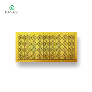
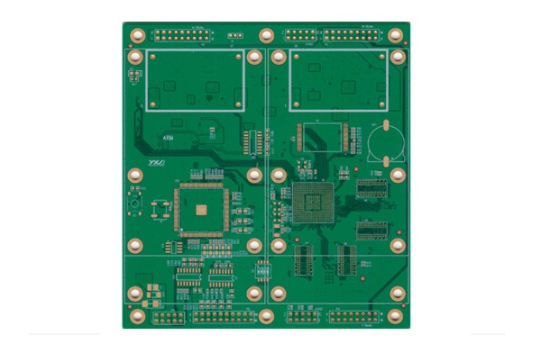
In anspruchsvollen Bereichen wie der Hochgeschwindigkeitskommunikation, der industriellen Steuerung und der High-End-Unterhaltungselektronik ist die 10-Lagen-Leiterplatte mit Durchgangsbohrung nimmt aufgrund seiner außergewöhnlichen Zuverlässigkeit, seiner hohen Belastbarkeit und seines ausgereiften Herstellungsverfahrens eine unersetzliche Stellung ein. Anders als HDI Bei der Blind/Buried-Via-Technologie werden bei durchkontaktierten Leiterplatten Löcher verwendet, die alle Schichten für elektrische Verbindungen durchdringen und eine solide physikalische Grundlage für komplexe Systeme bilden.
Inhaltsübersicht
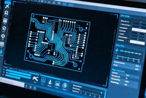
Technischer Kern von 10-Lagen-Durchsteck-Leiterplatten
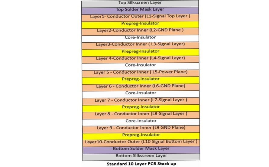
Das Wesentliche bei der Gestaltung eines 10-Lagen-Leiterplatte mit Durchgangsbohrung liegt in der Erzielung optimaler elektrischer Leistung und mechanischer Festigkeit durch eine präzise Stapelstruktur. Ein optimierter Lagenaufbau kontrolliert nicht nur effektiv die Impedanz, sondern verbessert auch die Signalintegrität und die elektromagnetische Verträglichkeit (EMV) erheblich.
Eine typische empfohlene Stapelstruktur sieht wie folgt aus:
| Reihenfolge der Ebenen | Ebene Typ | Primäre Funktion Beschreibung |
|---|---|---|
| 1 | Signalschicht | Oberste Schicht, für die Platzierung kritischer Komponenten und Hochgeschwindigkeitssignalleitungen. |
| 2 | Bodenebene | Bietet einen vollständigen Rückweg für Top- und Layer-3-Signale und schirmt Störungen ab. |
| 3 | Signalschicht | Bildet ein "Microstrip/Stripline"-Paar mit Layer 1 für optimale Signalqualität. |
| 4 | Signalschicht | Interne Signalweiterleitung. |
| 5 | Leistungsebene | Sorgt für eine stabile, rauscharme Stromversorgung der Chips. |
| 6 | Bodenebene | Trennt digitale/analoge Erdungen und stellt eine Referenz für die Stromversorgungsebene des Kerns bereit. |
| 7 | Signalschicht | Interne Signalweiterleitung. |
| 8 | Signalschicht | Bildet ein "Microstrip/Stripline"-Paar mit Schicht 10. |
| 9 | Bodenebene | Bietet eine Bezugsebene für Signale der unteren Schicht. |
| 10 | Signalschicht | Untere Schicht, für die Platzierung der Komponenten und die Signalverteilung. |
Wichtige Punkte beim Design:
- Impedanzkontrolle: Berechnen Sie die Leiterbahnbreite, die dielektrische Dicke und die Dielektrizitätskonstante genau, um die Kontinuität kritischer Impedanzen wie Differenzpaare (z. B. 100Ω) zu gewährleisten.
- Über Design: Es wird ein Lochdurchmesser von ≥ 0,2 mm empfohlen, und der Durchmesser des Pads sollte mindestens das 1,5-fache des Lochdurchmessers betragen, um eine gute mechanische Stabilität und elektrische Verbindung zu gewährleisten.
Verbesserung der Signalübertragungsstabilität
Die Stabilität der Signalübertragung ist entscheidend für den Erfolg eines 10-Lagen-Leiterplatte mit Durchgangsbohrung. Dies hängt von der richtigen Materialauswahl und fortschrittlichen Verarbeitungstechniken ab.
- Auswahl des Substrats: Für Hochgeschwindigkeits- oder Hochfrequenzanwendungen werden Laminate mit niedrige Dielektrizitätskonstante (Dk) und niedriger Verlustfaktor (Df) werden empfohlen, wie zum Beispiel Rogers RO4350B (Dk=3,48, Df=0,0037). Im Vergleich zu Standard-FR-4 kann es die Signaldämpfung um ein Vielfaches reduzieren.
- Kupfer-Folie Typ: Um die "Skin-Effekt"-Verluste bei hohen Frequenzen zu verringern, sollten Kupferfolien mit geringerer Oberflächenrauhigkeit gewählt werden, z. B. Gewalzte geglühte Kupferfolie (RACF) oder Sehr niedriges Profil (HVLP) Kupfer-Folie.
- Präzise Prozesse:
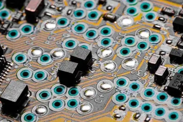
- Laserbohren: Erreicht eine Bohrgenauigkeit von ±5μm, sorgt für glatte Lochwände und reduziert Signalreflexionen.
- Einheitliche Beschichtung: Gleichmäßige Kupferdicke in den Löchern mit einer Toleranz von ±2μm, was eine gleichmäßige Stromübertragung gewährleistet.
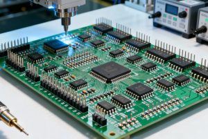
- AOI und Röntgeninspektion: Vollständige Qualitätsüberwachung des Prozesses zur Beseitigung potenzieller Fehler.
2025 Kosten-Tiefgang
Verstehen der Kostenstruktur von 10-Lagen-Leiterplatten mit Durchgangsbohrung ist für die Budgetierung und Kostenkontrolle von Projekten unerlässlich. Die Marktpreise von 2025 weisen unterschiedliche Merkmale auf.
1. Grundlegende Preisspanne:
- Standard FR-4 Material: Ungefähr 500 - 2.000 RMB/Quadratmeter.
- Kleinserie/Prototyp: Prototypen im Eilverfahren können bis zu 12,05 RMB pro Stück kosten.
- Hochfrequenz-/Spezialmaterialien: Zum Beispiel Rogers-Laminate, die 2.000 - 5.000 RMB/Quadratmeter kosten.
2. Tabelle zur Aufschlüsselung der Kernkosten:
| Kostenkategorie | Anteil | Wichtige Einflussfaktoren und Kostenschwankungen |
|---|---|---|
| Direkte Materialien | 40%-60% | - FR-4-Substrat: 0,3-0,8 RMB/cm² - Hochfrequenz-Material: 2-5 RMB/cm² - Kupferfolie: 3oz ist ~80% teurer als 1oz |
| Bearbeitungsgebühren | 30%-45% | - Die Kosten für das Laserbohren betragen das 2-3fache des mechanischen Bohrens - Der Energieverbrauch beim 10-Schicht-Mehrschichtlaminieren ist um 50% höher als beim 6-Schichtlaminieren. - Blind/Buried via Prozess fügt 30%-80% Kosten hinzu |
| Oberfläche | 5%-10% | ENIG > Bleifreies HASL > OSP (Kostensteigerung von links nach rechts) |
| Auftragsvolumen | Erhebliche Auswirkungen | Kosten für Chargen >50 ㎡ können 40%-60% niedriger sein als bei Prototypen |
3. Strategien zur Kostensenkung:
- Design-Optimierung: Eine Verringerung der Leiterbahnbreite auf ≥ 4mil und des Lochdurchmessers auf ≥ 0,2mm kann die Verarbeitungsschwierigkeiten und Kosten um 15%-25% reduzieren.
- Großeinkauf: Wenden Sie sich für die Produktion großer Mengen direkt an Fabriken in Regionen wie Jiangxi oder Dongguan, die erhebliche Preisvorteile bieten.
Durchlaufzeiten und Beschleunigungsstrategien im Überblick
Genaue Schätzung des Produktionszyklus für 10-Lagen-Leiterplatten mit Durchgangsbohrung ist entscheidend für die Projektplanung.
- Standard-Vorlaufzeit:
- Prototyping7-10 Arbeitstage.
- Massenproduktion: 10-15 Arbeitstage.
- Wichtige Einflussfaktoren:
- Entwurfskomplexität: Spezielle Anforderungen wie blinde/vergrabene Durchkontaktierungen und Impedanzkontrolle können 3-5 Tage in Anspruch nehmen.
- Auftragsvolumen: Kleine Chargen (<10 ㎡) können von Schnelldrehereien in 3-5 Tagen fertiggestellt werden; größere Mengen erfordern eine längere Planung.
- Strategien zur Verkürzung der Vorlaufzeit:
- Beschleunigte Dienste: Einige Hersteller aus Shenzhen (z. B. Junjiexin) bieten 24-Stunden-Prototyp im Eilverfahren Service, aber er kostet das 2-3fache des Standardpreises.
- Prozess- und Flussoptimierung: Durch den Einsatz von Laser Direct Imaging (LDI), die Optimierung des Plattendesigns und die Auswahl von Lieferanten mit fortschrittlicher Ausrüstung (z. B. sind Lieferanten aus Shenzhen oft 1-2 Tage schneller) kann der Gesamtzyklus auf 5-7 Tage verkürzt werden.
Wie man eine Qualität auswählt PCB-Hersteller?
Die Wahl des richtigen Herstellers ist der Schlüssel zum Projekterfolg. Hier sind die wichtigsten Kriterien für die Bewertung von Lieferanten:
1. Bewertung der technischen Leistungsfähigkeit:
- Ausstattung Level: Gibt es hochpräzise Laserbohrmaschinen, LDI-Belichtungssysteme usw.?
- Prozess-Erfahrung: Haben sie Erfahrung mit der Massenproduktion von 10-Lagen-Platinen, insbesondere im Hinblick auf Impedanzkontrolle und zuverlässige Beschichtungsmöglichkeiten?
2. Zertifizierung des Qualitätssystems:
- Muss haben IPC-6012 (Qualifikations- und Leistungsspezifikation für starre Leiterplatten) und ISO 9001 Zertifizierungen.
- Überprüfen Sie für den Bereich Automobil/Militär Zertifizierungen wie IATF 16949.
3. Checkliste für die Lieferantenauswahl:
| Dimension der Bewertung | Bevorzugte Aktion | Risikovermeidung |
|---|---|---|
| Geografischer Standort | Bevorzugen Sie PCB-Industriecluster für eine schnelle Reaktion der Lieferkette. | Vermeiden Sie Händler ohne physische Fabriken. |
| Kunden-Fallstudien | Erbitten Sie Erfolgsgeschichten in relevanten Bereichen (z. B. Basisstationen, industrielle Steuerung). | Seien Sie misstrauisch gegenüber Verkäufern, die keine Nachweise erbringen können. |
| Technische Unterstützung | Bestätigen Sie die Verfügbarkeit von Mehrwertdiensten wie DFM-Überprüfung und Impedanzberechnung. | Reine OEM-Modelle ohne technische Unterstützung werden abgelehnt. |
Empfehlung: Vor der endgültigen Entscheidung sollten 5-10 Testplatinen hergestellt werden, um wichtige Aspekte wie die Kupferdicke in den Löchern (≥25μm) und die Passgenauigkeit von Schicht zu Schicht zu überprüfen und die Bedingungen für Qualitätsansprüche im Vertrag zu klären.
Anwendungsszenarien und zukünftige Trends
10-Lagen-Leiterplatten mit Durchgangsbohrung spielen aufgrund ihrer überragenden Stabilität und ihrer Fähigkeit zur Zusammenschaltung mit hoher Dichte eine zentrale Rolle in den folgenden Bereichen
- Industrielle Kontrollsysteme: Sie erfordern eine extrem hohe mechanische und thermische Zuverlässigkeit in rauen Umgebungen.
- Basisstation Kommunikationsausrüstung: Bewältigung komplexer Signale und Hochfrequenzübertragungen, die eine hervorragende Signalintegrität erfordern.
- Hochwertige Unterhaltungselektronik: Zum Beispiel Server, High-End-Grafikkarten, die ein Gleichgewicht zwischen Leistung, Kosten und Wärmemanagement erfordern.
Mit den Fortschritten in der Materialwissenschaft und den Herstellungsverfahren, 10-Lagen-Leiterplatten mit Durchgangsbohrung entwickeln sich in Richtung höherer Frequenzen, höherer Leistungsdichte und besserer Wärmemanagementleistung weiter und bieten eine solide Hardwareplattform für elektronische Geräte der nächsten Generation.