Wie hoch sind die Kosten für die Herstellung einer mehrlagigen Leiterplatte?
Inhaltsübersicht
Multidimensionale Analyse der PCB-Kostenstruktur
Als zentraler Träger elektronischer Systeme werden die Herstellungskosten von Leiterplatten von einer Vielzahl von Faktoren beeinflusst, darunter Materialien, Prozesse, Designkomplexität und Menge. Nach dem IPC-6012-Standard kann die Kostenstruktur moderner Leiterplatten in die folgenden Schlüsseldimensionen unterteilt werden:
Der konkrete Preis ist Gegenstand der aktuellen Mitteilung.
1. Kosten des Substrats (25-40% der Gesamtkosten):
- Standard FR-4 Epoxid-Glasgewebe-Substrat: ¥50-150/m²
- Hochfrequenzmaterialien (z. B. Rogers RO4003C):¥800-2000/m²
- Hoch-TG-Materialien (TG170+): 30-50% höher als Standard FR-4
- Aluminium-Substrat (IMS): ¥300-800/m²
2. Kupferfolienkosten (15-25% der Gesamtkosten):
- Standard 1oz (35μm) elektrolytische Kupferfolie: Grundpreis
- 2 Unzen Kupferfolie: 35-40% Kostensteigerung
- 3 Unzen+ dickes Kupfer: Exponentielles Kostenwachstum
3. Prozesskosten (30-45% der Gesamtkosten):
- Standardverfahren für durchkontaktierte Leiterplatten: Grundlegende Kosten
- Blind/begraben durch Verfahren:20-30% Kostensteigerung
- HDI-Verfahren (High Density Interconnect):50-100% Kostensteigerung
- Anforderungen an die Impedanzkontrolle:15-25% zusätzliche Kosten
Auf der Suche nach kostengünstigen PCB-Lösungen? Erhalten Sie ein sofortiges, auf Ihre Projektanforderungen zugeschnittenes Angebot!
Quantitative Analyse der Auswirkungen der Lagenzahl auf die Kosten
Die Beziehung zwischen PCB-Lagen und Kosten zeigt nichtlineares Wachstumdie durch die folgenden technischen Faktoren bestimmt werden:
| Schichten | Kostenfaktor | Wichtige technische Herausforderungen |
|---|---|---|
| 1-2 | 1.0x | Grundlegendes Verfahren, Ausbeute >95% |
| 4 | 1.8-2.2x | Ausrichtungsgenauigkeit der Laminierung ±50μm |
| 6 | 2.5-3.0x | AOI-Inspektion der Innenschicht erforderlich |
| 8 | 3.5-4.5x | Kontrolle der dielektrischen Gleichmäßigkeit zwischen den Schichten |
| 10+ | 5.0x+ | Erfordert ein segmentiertes Laminierungsverfahren |
Bemerkenswert, 4-6 Schichtplatten bieten das beste Preis-Leistungs-Verhältnis in der Unterhaltungselektronik, wobei Kostensteigerungen in erster Linie aus:
- Zusätzliche Laminierungsschritte (jede Laminierung kostet ¥15-25/m²)
- Geringere Ausbeute bei der Übertragung von Mustern auf die Innenschicht (typischerweise 85-90 % gegenüber 95 % und mehr auf der Außenschicht)
- Höhere Anforderungen an die Bohrgenauigkeit (die Genauigkeit der Lochposition muss innerhalb von ±25μm liegen)
Kostenprämienanalyse fortgeschrittener Prozesse
Moderne Elektronik erfordert hohe Leistung und Zuverlässigkeit aus PCBs, mit den damit verbundenen speziellen Verfahren, die sich wie folgt auf die Kosten auswirken:
- HDI-Technik (High Density Interconnect):
- Laserbohren (¥0,002-0,005/Loch) gegenüber mechanischem Bohren (¥0,0005-0,001/Loch)
- Beliebige Layer-Verbindungsstrukturen erhöhen die Kosten um 80-120%.
2. Hochfrequenz-Materialbearbeitung:
- PTFE-Materialien erfordern spezielle Bohrparameter, die die Verarbeitungseffizienz um 30 % verringern
- Oberflächenbehandlung erfordert ENIG (Chemisch Nickel Tauchgold), 60% teurer als HASL
3. Hohe Zuverlässigkeitsanforderungen:
- IPC Klasse 3 Normen erhöhen die Kosten um 20-30%
- 100%ige Abdeckung durch elektrische Tests führt zu zusätzlichen Kosten von 8-12%.
- Luft- und Raumfahrttaugliche Reinigungsverfahren erhöhen die Behandlungskosten um 15-20%.
Technische Praktiken zur Kostenoptimierung
Basierend auf Entwurf für Six Sigma (DFSS) Prinzipien schlagen wir die folgenden Strategien zur Kostenoptimierung vor:
- Optimierung der Entwurfsphase:
- Rationelle Auswahl der Lagenzahl (durch Simulation verifiziert)
- Optimierte Routingregeln (Reduzierung des speziellen Impedanzleitungsverhältnisses)
- Standardisierte Öffnungsgrößen (reduziert die Häufigkeit des Bohrerwechsels)
2. Strategie der Materialauswahl:
- Hybrides Materialdesign (kritische Schichten aus Hochleistungsmaterialien)
- Optimierung der Kupferdicke (genau berechnet auf Basis der aktuellen Belastung)
- Auswahl der Oberflächenbehandlung (Unterhaltungselektronik kann OSP anstelle von ENIG verwenden)
3. Kontrolle des Herstellungsprozesses:
- Umsetzung der statistischen Prozesskontrolle (SPC) zur Verbesserung der Ausbeute
- Anwendung des Managements der Gesamtanlageneffektivität (OEE)
- Einführung von Systemen für Qualitätsingenieure für Lieferanten (SQE)
Sind Sie bereit, Ihre PCB-Kosten zu optimieren? Unser Team hat Kunden geholfen, durchschnittlich 22 % ihrer PCB-Kosten einzusparen. Beginnen Sie mit einer kostenlosen Beratung!
Prognose der Kostenentwicklung in der Industrie
Laut Prismark-Industrieberichten werden die PCB-Kosten in den nächsten 5 Jahren folgende Entwicklungstrends aufweisen:
- Werkstoff-Innovation:
- Die Lokalisierung von verlustarmen Materialien wird die Preise um 20-30% senken
- Neue Harzsysteme können die Kosten für Hochfrequenzplatten um 40 % senken
2. Prozess-Fortschritte:
- Die Direct Imaging (DI)-Technologie wird die Lithografiekosten um 15% senken
- Intelligente Fertigung wird die Arbeitskosten auf unter 8% senken
3. Design-Revolution:
- Die 3D-Drucktechnologie wird die Kostenstruktur von Kleinserien-Leiterplatten verändern
- Technologie für eingebettete Komponenten kann die Gesamtsystemkosten um 25 % senken
Topfast’s Vorteile bei der Herstellung von Mehrschichtplatten
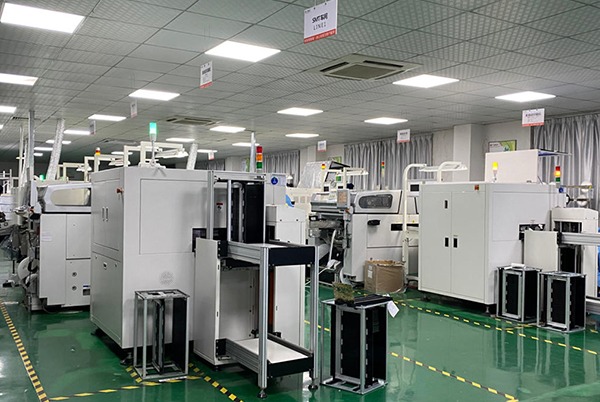
Gegründet im Jahr 2008, Topfast ist ein führender Hersteller von Leiterplattendesign, Fertigung und Montage mit 17 Jahren Erfahrung. Als Anbieter von Leiterplattenlösungen aus einer Hand sind wir darauf spezialisiert, Kunden mit Bedarf an Rapid Prototyping und Kleinserienfertigung zu bedienen.
Wir sind mit modernsten Produktionsanlagen ausgestattet (u.a. Laserbohrmaschinen, VCP via Fülllinien, Blind via AOI (z. B. Inspektionsgeräte, Keramikschleifanlagen, vertikale Vakuum-Harzverschließmaschinen usw.), ein erstklassiges technisches Team, ausgereifte Produktlinien und ein umfassender Serviceprozess, der es uns ermöglicht, unseren Kunden verschiedene maßgeschneiderte Dienstleistungen anzubieten. Das Unternehmen führt kontinuierlich neue Geräte, Technologien und hochwertige Materialien ein, um die Qualität der PCB-Produkte zu gewährleisten.
Wir pflegen enge Partnerschaften mit führenden Komponentenherstellern, um sowohl eine hervorragende Qualität der Komponenten als auch wettbewerbsfähige Preise zu gewährleisten.Unser 24/7-Kundendienstteam steht Ihnen bei allen Problemen zur Verfügung. Sie können sich mit unseren Kundendienstmitarbeitern vor Ort in Verbindung setzen, um auf Ihre E-Mails oder Nachrichten zu antworten. Von dem Moment an, in dem Sie Ihre Gerberdateien einreichen, bis Sie Ihre Leiterplatte und die bestückte Leiterplatte zu Ihrer Zufriedenheit erhalten, wird unser Serviceteam Ihre Bestellung während des gesamten Prozesses überwachen.


Verwandte Beiträge