PCB-kokoonpano (PCBA) on vaihe, jossa paljaasta PCB:stä tulee toimiva elektroniikkalevy.PCB-valmistus keskittyy paljaan levyn valmistusvaiheeseen, joka muodostaa perustan koko PCB-valmistuksen työnkululle. Siihen kuuluu komponenttien sijoittelu, juottaminen ja tiukka testaus.
Kokoonpanon laatu vaikuttaa suoraan:
- Sähköinen toimivuus
- Tuotteen luotettavuus
- Valmistuksen tuotto
Osoitteessa TOPFAST, kokoonpanoa käsitellään saantoon perustuva prosessi, varmistaen, että levyt ovat toimivia ja vankkoja.
Taustatietoa siitä, miten piirilevyjen kokoonpano liittyy valmistukseen, löydät osoitteesta: PCB Fabrication vs PCB Assembly
Sisällysluettelo
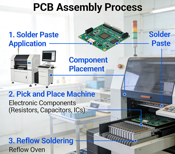
Pinta-asennustekniikka (SMT) kokoonpano
Mikä on SMT-kokoonpano?
SMT-kokoonpanossa asennetaan pinta-asennettavat komponentit suoraan piirilevyn tyynyihin käyttämällä:
- Juotospasta
- Pick-and-place-koneet
- Reflow-juottaminen
SMT on nopea, tarkka ja soveltuu suuritiheyksisille levyille., jota käytetään yleisesti kulutuselektroniikassa, televiestinnässä ja IoT-laitteissa.
SMT-haasteet
- Hienojakoiset komponentit vaativat äärimmäistä sijoitustarkkuutta
- Lämpöjännitys uudelleenjuoksutuksen aikana voi vahingoittaa piirilevyjä, jos sisäkerrokset tai kuparointi ovat epäjohdonmukaisia.
- Suuritiheyksiset levyt lisäävät tuottoherkkyyttä
TOPFASTissa SMT-kokoonpano koordinoidaan huolellisesti valmistustietojen kanssa, jotta minimoida viat ja parantaa tuottoa.
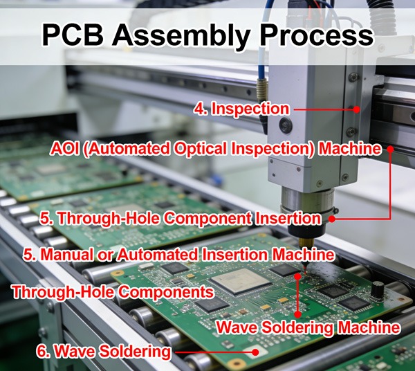
Läpivientireiän kokoonpano
Mikä on läpivientireikäasennus?
Läpireikäkokoonpano lisää komponentit johdoilla porattuihin reikiin ja juotetaan käyttäen:
- Aaltojuottaminen (massajuottaminen)
- Manuaalinen juottaminen (prototyypeille tai pienen sarjan levyille)
Läpireikää käytetään edelleen laajalti:
- Mekaaninen lujuusN/OFF)
- Suuritehoiset komponentit
- Liittimet ja suuret pakkaukset
Läpivientireiän kokoonpanon työnkulku
- Reikien täyttö / komponenttien lisääminen - Aseta komponenttien johdot pinnoitettuihin reikiin
- Juottaminen - Aalto- tai valikoiva juottaminen kiinnittää komponentit paikoilleen
- Tarkastus - Juotoslaadun visuaaliset tai AOI-tarkastukset
Poraus- ja pinnoitustyön laatuun vaikuttavat suoraan seuraavat tekijät PCB-poraus vs. laserporausja Kuparointiprosessi selitetty.
Läpivientireikien haasteet
- Väärin kohdistetut tai huonosti pinnoitetut reiät vähentävät juotosliitoksen luotettavuutta.
- Manuaalinen kokoonpano lisää työvoimakustannuksia ja inhimillisten virheiden mahdollisuutta.
- Vaatii enemmän levyn kiinteää tilaa kuin SMT
TOPFAST yhdistää tarkkuusporaus ja pinnoitus kokoonpanon optimoinnin avulla maksimoimaan reikien läpivientituotto.
Kokoonpanon testaus ja laadunvalvonta
Piirin sisäinen testaus (ICT)
ICT-tarkastukset
- Shortsit
- Avaa
- Oikeat komponenttien arvot
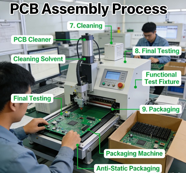
Toiminnallinen testaus
Toiminnallisessa testauksessa simuloidaan reaalimaailman toimintaa, jotta voidaan varmistaa, että piirilevy toimii suunnitellulla tavalla.
Testaus on viimeinen tarkastuspiste, jolla varmistetaan, että valmistus- ja kokoonpanovaiheet täyttävät eritelmät. Katso Syövytysprosessi ja saannon valvonta selitetty miten varhaisvaiheen laatu vaikuttaa testauksen tuloksiin.
Kokoonpanon tuottoa koskevat näkökohdat
Tuotto
- Valmistuksen laatu (esim. sisäkerrokset, poraus, pinnoitus).
- Komponenttien sijoittelun tarkkuus
- Juotosparametrit
- Piirilevysuunnittelu (lämpö, etäisyys, tyynyjen koko)
Korkean tuoton kokoonpano vähentää:
- Uudelleen työstäminen
- Romu
- Tuotannon kokonaiskustannukset
- Katso PCB Fabrication vs PCB Assembly miten saantoa koskevat näkökohdat kattavat molemmat prosessit.
Kokoonpanon kustannustekijät
Keskeiset kustannustekijät:
- Komponentin tyyppi ja pakkaus
- Levyn tiheys ja kerrosluku
- Kokoonpanovolyymi (prototyyppi vs. massatuotanto)
- Testaus- ja tarkastusvaatimukset
Kokoonpanon optimointi laadusta tinkimättä edellyttää suunnittelu-, valmistus- ja kokoonpanoprosessien tiivis yhteensovittaminen..
Päätelmä
PCB-kokoonpano muuntaa paljaan levyn täysin toimivaksi elektroniseksi tuotteeksi.
SMT- ja läpireikäprosessitYhdessä vankan testauksen kanssa ne määrittelevät lopputuotteen luotettavuuden.
Integrointi valmistuksen laatuun on olennaisen tärkeää:
- Korkea tuotto
- Kustannustehokas tuotanto
- Pitkäaikainen luotettavuus
PCB-kokoonpanoprosessin usein kysytyt kysymykset
V: Piirilevykokoonpanoon kuuluu elektronisten komponenttien asentaminen valmistetulle piirilevylle SMT- tai läpivientitekniikalla, minkä jälkeen suoritetaan tarkastus ja testaus.
V: SMT asentaa komponentit piirilevyn pinnalle, kun taas läpivientireikä asettaa komponenttien johtimet porattuihin reikiin ja juottaa ne.
V: Väärin kohdistetut kerrokset, huonosti poratut reiät tai epäjohdonmukainen pinnoitus voivat aiheuttaa juotosvirheitä ja vähentää kokoonpanon tuottoa.
A: Automaattinen optinen tarkastus (AOI), röntgentarkastus, piirin sisäinen testaus (ICT) ja toiminnallinen testaus ovat yleisesti käytettyjä.
V: TOPFAST yhdenmukaistaa valmistus- ja kokoonpanoprosessit, soveltaa automaattisia ja manuaalisia tarkastuksia ja käyttää saantoon perustuvaa optimointia luotettavan tuotannon varmistamiseksi.