Home >
Blog >
notizie > Come risolvere i problemi di sovrapposizione tra maschera di saldatura e strati serigrafici nella progettazione di PCB
In TOPFAST Progettazione PCB esperienza di revisione e produzione, sovrapposizione tra la maschera di saldatura e gli strati serigrafici è uno dei problemi di progettazione più comuni che può portare a difetti di saldatura e compromettere l'affidabilità del prodotto. Affrontare adeguatamente questo problema è fondamentale per garantire la producibilità del PCB e la qualità finale.
Rischi fondamentali derivanti da problemi di sovrapposizione
- Rischi per la qualità della saldatura
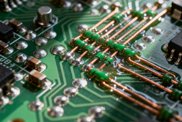
L'inchiostro serigrafico è isolante. Se copre le piazzole di saldatura, ostacola direttamente l'efficace legame tra la saldatura e lo strato di rame. Questo può portare a giunzioni di saldatura fredde, resistenza insufficiente del giunto di saldatura o saldatura incompleta, potenzialmente in grado di provocare guasti durante le prove di vibrazione o di ciclismo ad alta/bassa temperatura.
- Conflitti del processo di produzione
Nel processo di produzione dei PCB, lo strato della maschera di saldatura ha solitamente la priorità del processo. L'inchiostro serigrafico nelle aree che si sovrappongono può essere inciso o parzialmente rimosso, dando luogo a caratteri incompleti, sfocati o disallineatiche influisce sull'accuratezza dell'assemblaggio e sulle successive operazioni di riparazione e debugging.
- Riduzione della professionalità del prodotto
Una serigrafia disordinata e sovrapposta non solo riduce la leggibilità del circuito stampato, ma riflette anche una svista nella fase di progettazione, con un impatto sull'immagine complessiva del prodotto.
Soluzioni sistematiche consigliate da TOPFAST
I. Impostazione di regole preventive
- Impostazioni delle regole chiave:
In strumenti EDA come Altium Designer o Allegro, è fondamentale stabilire la "Distanza tra seta e maschera di saldatura". regola. TOPFAST raccomanda:- Disegni generali: Distanza minima ≥ 0,15 mm (6mil)
- Progetti ad alta densità: Può essere negoziato fino a 0,1 mm (4mil)ma la capacità di processo deve essere confermata in anticipo.
- Schede ad alta frequenza/alta tensione: Raccomandare ≥ 0,2 mm (8mil) per garantire un passaggio sicuro
- Esempio di implementazione di una regola (Altium Designer):
Design → Regole → Produzione → SetaPerSaldareMascheraClearance- Impostare gli oggetti corrispondenti (Primo oggetto: livello Seta; Secondo oggetto: livello Maschera di saldatura)
- Eseguire un'analisi completa Controllo delle regole di progettazione (RDC) dopo aver applicato la regola
II. Verifica del progetto e perfezionamento del manuale
- Ispezione visiva della pila di strati:
Nell'editor di PCB, visualizzare solo la sezione strato di serigrafia + strato di maschera di saldatura/pad e utilizzare il contrasto cromatico per identificare visivamente le aree che si sovrappongono.
- Elaborazione ad anello chiuso degli errori DRC:
Esaminare e regolare manualmente ogni punto di sovrapposizione segnalato dal DRC, tra cui:- In movimento/rotazione posizioni dei caratteri
- Semplificare marcature non essenziali (conservare solo i designatori, la polarità e le etichette di interfaccia)
- Standardizzazione orientamento dei caratteri e dimensione dei caratteri (larghezza/altezza della linea consigliata di 5/30mil)
III. Raccomandazioni di collaborazione produttiva con TOPFAST
- Confermare i dettagli del processo in anticipo
Prima di inviare i file della scheda, fornire i file di progetto a TOPFAST per un Revisione del Design for Manufacturability (DFM). Forniremo un feedback su:- Parametri ottimali di spaziatura tra maschera serigrafica e maschera di saldatura per il vostro design
- Suggerimenti per la regolazione del processo per materiali specifici/finiture superficiali
- Soluzioni di ottimizzazione della serigrafia per aree ad alta densità
- Utilizzate il principio della "priorità della maschera di saldatura".
Durante la produzione, TOPFAST si attiene rigorosamente al principio di "L'accuratezza dell'apertura della maschera di saldatura ha la priorità sull'integrità della serigrafia". per garantire che i tamponi rimangano assolutamente puliti. Si raccomanda di trattare serigrafia attiva evitare le pastiglie come regola ferrea durante la progettazione.
- Output di progettazione standardizzato
Si consiglia di consegnare i file in IPC-2581 o Formato Gerber X2 con descrizioni delle proprietà dei livelli per ridurre gli errori di interpretazione in fase di produzione.
Tabella di riferimento delle capacità di processo TOPFAST
| Tipo di design | Distanza consigliata tra seta e maschera di saldatura | Supporto al processo TOPFAST | Osservazioni |
|---|
| Elettronica di consumo generale | ≥0,15 mm (6mil) | Supporto standard | Compatibile con la maggior parte delle applicazioni commerciali |
| Interconnessione ad alta densità (HDI) | ≥0,1 mm (4mil) | Richiede una revisione preventiva | In combinazione con il processo di imaging laser LDI |
| Grado automobilistico/industriale | ≥0,2 mm (8mil) | Garanzia di priorità | Soddisfa i requisiti di affidabilità più elevati |
| PCB flessibile (FPC) | ≥0,15 mm (6mil) | Adattamento dell'inchiostro speciale | Impedisce che la serigrafia si screpoli nelle aree di piegatura |
conclusioni
Noi di TOPFAST crediamo che "La progettazione determina il tetto di produzione". Per quanto riguarda il problema della sovrapposizione tra la maschera di saldatura e gli strati di serigrafia, si consiglia di:
- Lato design: Applicare rigorosamente le regole di autorizzazione e utilizzare gli strumenti DRC per eliminare i rischi all'origine della progettazione.
- Lato recensione: Utilizzare la funzione TOPFAST strumento di ispezione DFM online gratuito o sottoporre i file alla revisione di un esperto per ottenere raccomandazioni personalizzate.
- Lato produzione: Etichettare chiaramente i requisiti di spazio libero per le aree critiche e selezionare i parametri di progettazione che corrispondono alle capacità di processo di TOPFAST.
Attraverso la duplice garanzia di prevenzione progettuale + collaborazione produttivaTOPFAST aiuta a eliminare "problemi minori" come la sovrapposizione delle serigrafie, migliorando la resa al primo passaggio dei PCB e l'affidabilità dei prodotti finali.
Avete bisogno che TOPFAST vi fornisca raccomandazioni su misura per le regole di autorizzazione alla serigrafia per il vostro progetto?
Non esitate a caricare i file del vostro design o a contattarci per un Rapporto di analisi DFM gratuito. Forniamo soluzioni di ottimizzazione basate sulle reali capacità produttive.
Problemi fondamentali comuni nella progettazione delle maschere di saldatura dei PCB
Nella produzione di PCB, la progettazione delle maschere di saldatura ha un impatto diretto sull'affidabilità e sulla resa del prodotto. Sulla base dell'esperienza di produzione, TOPFAST riassume i cinque problemi più comuni di progettazione delle maschere di saldatura, oltre alla sovrapposizione della serigrafia, con le relative soluzioni:
D: Larghezza insufficiente della diga della maschera di saldatura A: Problema: L'isolamento della maschera di saldatura tra le piazzole adiacenti è troppo stretto (<0,08 mm) e tende a rompersi durante la produzione.
Il rischio: Ponti di saldatura e cortocircuiti, in particolare per i componenti 0402/0201 e i chip QFN.
Soluzione:
Design standard: Maschera di saldatura ≥ 0,08mm (3mil)
Design ad alta densità: ≥ 0,05mm (2mil), soggetto a conferma di processo
Per aree ultra-dense come BGA: fornire soluzioni di ottimizzazione della maschera di saldatura localizzata
D: Dimensioni errate dell'apertura della maschera di saldatura Problema: La dimensione dell'apertura non corrisponde alla piazzola: troppo piccola influisce sulla saldabilità, troppo grande espone le tracce.
Specifiche TOPFAST:
Design standard: L'apertura si estende per 0,05-0,1 mm (2-4mil) oltre il cuscinetto per ogni lato.
Pad BGA: Si consiglia di utilizzare piazzole con maschera di saldatura definita (SMD).
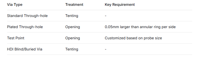
D: Trattamento improprio della maschera di saldatura della via A: Problema: Scelta errata tra apertura o tenda, che influisce sulla saldatura e sull'isolamento.
Strategia di trattamento:
D: Progetto con tolleranza di allineamento insufficiente A: Problema: Se non si tiene conto delle deviazioni di allineamento della produzione, la maschera di saldatura può coprire i bordi delle piazzole.
Principio: Implementare il design "copper pullback" per tutte le aperture per garantire che le piastre siano completamente esposte in condizioni di massima deviazione del processo.
D: Trascurare la progettazione di aree speciali A: Trattamenti dell'area chiave:
Bordo scheda/V-CUT: La maschera di saldatura non deve coprire le linee di separazione
Dita d'oro: Non è assolutamente consentita la copertura della maschera di saldatura
Tracce ad alta frequenza: È possibile utilizzare la rimozione locale della maschera di saldatura o un inchiostro a basso Dk/Df.
Raccomandazione TOPFAST: Verifica del progetto in quattro fasi
Impostazione delle regole: Stabilire set di regole per la progettazione di maschere di saldatura negli strumenti EDA
Ispezione visiva: Generazione di viste di controllo dello strato di maschera di saldatura dedicate
Analisi DFM: Utilizzate lo strumento online gratuito TOPFAST per il pre-check.
Ottimizzazione del design: Iterare le aree critiche in base ai risultati dell'analisi
Avete bisogno di regole complete per la progettazione di maschere di saldatura o DFM recensione?
Caricate i file di progettazione su TOPFAST per ottenere soluzioni personalizzate basate sull'esperienza di produzione.