I difetti di produzione dei PCB sono raramente casuali.
La maggior parte dei difetti ha origine da decisioni di progettazione, limitazioni dei materiali o instabilità del processo, molto prima che avvenga l'ispezione finale.
Mentre l'ispezione può rilevare molti problemi visibili, la prevenzione dei difetti deve avvenire nelle prime fasi del processo produttivo.
Questo articolo illustra i più comuni difetti di produzione dei PCB, le loro cause principali e le strategie pratiche di prevenzione dal punto di vista della produzione.
Per i fondamenti della qualità, vedere: Cosa determina la qualità dei PCB?
Indice per materie
Cosa si intende per difetto di produzione di un PCB?
Un difetto di fabbricazione di un PCB è una qualsiasi deviazione che:
- Influenza le prestazioni elettriche
- Compromette l'integrità meccanica
- Riduce l'affidabilità a lungo termine
- Violazione delle specifiche IPC o del cliente
I difetti possono essere visibile, latente, o progressivoche compaiono solo in seguito a sollecitazioni termiche o meccaniche.
Difetti dello strato interno
Difetti comuni dello strato interno
- Circuiti aperti
- Cortocircuiti
- Sovra-incisione o sotto-incisione
- Disregistrazione tra gli strati
Cause principali
- Imprecisioni di imaging
- Variazione del processo di incisione
- Scarso allineamento dello strato interno
Poiché gli strati interni vengono sigillati durante la laminazione, i difetti in questa fase sono irreversibile.
Sfondo del processo: Spiegazione della fabbricazione dello strato interno
Difetti legati alla perforazione
Difetti tipici di perforazione
- Fori decentrati
- Bave e sbavature
- Punte da trapano rotte
- Scarsa qualità della parete del foro
Cause principali
- Rapporto d'aspetto eccessivo della punta
- Utensili usurati
- Avanzamento e velocità non corretti
- Metodo di perforazione inadeguato
I difetti di foratura influiscono direttamente sulla qualità della ramatura e sull'affidabilità della via.
Confronto dei metodi:
Foratura di PCB vs foratura laser
Difetti di placcatura
Problemi comuni di placcatura
- Rame sottile nei vias
- Vuoti o lacune
- Rame ruvido o nodulare
- Scarsa adesione
Cause principali
- Preparazione della superficie non corretta
- Densità di corrente incoerente
- Squilibrio chimico
- Vias ad alto rapporto d'aspetto
I difetti di placcatura sono una delle principali cause di guasti intermittenti e i problemi legati ai cicli termici.
Dettaglio del processo: Processo di ramatura nella produzione di PCB
Difetti di incisione
Difetti tipici dell'incisione
- Tracce sovraincise
- Ponti di rame sotto-incisi
- Variazione della larghezza della linea
- Traccia del collo
Cause principali
- Spessore del rame non uniforme
- Chimica aggressiva del mordente
- Scarsa compensazione dei processi
- Spaziatura stretta tra le tracce
Man mano che la geometria delle tracce diventa più fine, i difetti di incisione incidono sempre più sulla resa e sull'affidabilità.
Analisi incentrata sul rendimento: Processo di incisione dei PCB e controllo della resa
Difetti di laminazione e delaminazione
Problemi comuni di laminazione
- Delaminazione
- Vesciche
- Vuoti di resina
- Spostamento di livello
Cause principali
- Pressione o temperatura di laminazione non corretta
- Scarsa selezione del prepreg
- Assorbimento dell'umidità
- Accatastamenti sbilanciati
Questi difetti spesso si manifestano durante l'assemblaggio o i cicli termici, piuttosto che durante i test iniziali.
Relazione materiale: Costo del materiale e degli strati del PCB
Difetti della maschera di saldatura e della finitura superficiale
Difetti tipici
- Disallineamento della maschera di saldatura
- Scarsa adesione
- Fori di spillo
- Spessore della finitura superficiale non uniforme
Cause principali
- Preparazione inadeguata della superficie
- Condizioni di polimerizzazione non corrette
- Contaminazione del processo
Questi difetti possono causare ponti di saldatura, corrosione e riduzione della durata di conservazione.
Fughe di test elettrici e difetti latenti
Non tutti i difetti vengono rilevati durante i test elettrici.
I difetti latenti possono:
- Superare i test iniziali
- Cedimento in seguito a stress termico
- Appaiono durante le operazioni sul campo
Le cause più comuni includono:
- Spessore marginale della placcatura
- Microfessure nei vias
- Formazione di CAF
Rischi di difetti di progettazione
Alcuni difetti derivano da scelte progettuali piuttosto che da errori di produzione.
I fattori di progettazione ad alto rischio includono:
- Tracce e spaziature estremamente sottili
- Vias ad alto rapporto d'aspetto
- Distribuzione in rame non bilanciata
- Tolleranze troppo strette
Connessione di qualità progettuale: Fattori di costo della progettazione di PCB
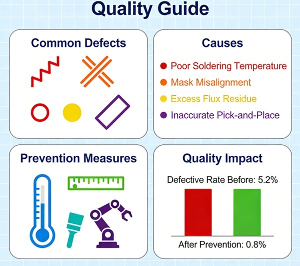
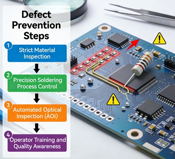
Come prevenire i difetti di produzione dei PCB
Una prevenzione efficace dei difetti si concentra su stabilità del processo, non solo l'ispezione.
Le principali strategie di prevenzione comprendono:
- Revisione precoce del DFM
- Margini di progettazione conservativi
- Selezione di materiali qualificati
- Monitoraggio della capacità di processo
- Analisi dei dati di resa
In TOPFAST, la prevenzione dei difetti è guidata da controllo del processo a monte e feedback basato sui datiriducendo la dipendenza dallo screening di fine linea.
Prevenzione dei difetti e costi di produzione
La prevenzione dei difetti spesso riduce il costo totale.
I vantaggi includono:
- Rendimento più elevato
- Meno lavoro di rielaborazione
- Meno ritardi
- Riduzione del rischio di guasto del campo
Equilibrio tra costi e qualità: Spiegazione dei costi di produzione dei PCB
conclusioni
I difetti di produzione dei PCB sono raramente incidenti isolati.
Sono il risultato di interazioni tra progettazione, materiali e controllo del processo.
Comprendendo i tipi di difetti più comuni e le loro cause principali, gli ingegneri e gli acquirenti possono adottare misure proattive per prevenire i difetti e migliorare l'affidabilità a lungo termine.
Questo articolo costituisce un pilastro fondamentale del Qualità e affidabilità dei PCB cluster.
FAQ: Difetti di produzione dei PCB
R: I difetti legati all'incisione e i problemi di placcatura sono tra i più comuni.
R: No. L'ispezione rileva i difetti ma non ne previene le cause.
R: Le sollecitazioni termiche durante l'assemblaggio possono rivelare difetti latenti introdotti in precedenza.
R: No. Molti difetti derivano dalla progettazione o dalla scelta dei materiali.
R: Attraverso la revisione DFM e una progettazione conservativa allineata alla capacità del processo.