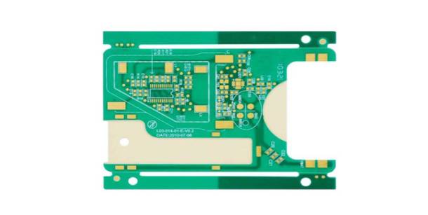
What is high speed? This is the basis for considering the high speed problem, and is also a problem among many hardware engineers. With the development of the times, electronic design engineers have slowly reached a consensus.
The edge rate of the signal is the key to determine the high-speed problem. When the signal's rise time and transmission delay can be compared, it is a high-speed circuit. Although there are various circuits on the PCB, there are always some general principles that can be observed for the design. Rigid PCB Manufacturersto explain.
1. Impedance matching principle
Impedance mismatch is the root cause of many high-speed problems caused by reflections. Conventionally, a high-speed problem cannot be discussed without an impedance match. From this design original. The following high-speed PCB board design requirements are derived:
(1) A reasonable layout for termination matching design. In PCB layout, first determine the position of electronic components on the PCB, then design the power line, ground line and high-speed signal line
After the design of ordinary signal lines.
(2) Less through holes, which will cause important impedance discontinuity.
(3) The stacking setting is reasonable to ensure that the impedance is consistent after the signal is changed, while taking into account the performance and price.
(4) Pay attention to the corners of the trace. 900 and acute angles will cause impedance discontinuities.
(5) The line width is equal, and the line width can be partially reduced in the range of BGA (PCB with ball grid array structure) and high-speed connectors. These areas are also impedance discontinuities.
(6) Differential wiring is equally spaced to control differential impedance.
(7) Pay attention to the signal cross-segmentation. In addition to the problem of backflow, the position of the cross-segmentation is also a point of impedance discontinuity.

High Speed PCB
2. Principle of suppressing interference
Interference includes the mutual interference of wiring and components inside the board, as well as the interference of the external electromagnetic environment.
(1) Route 3W principle to ensure line spacing.
(2) The 20H criterion suppresses signal radiation outside the board.
(3) When possible, minimize the distance between the signal layer and the reference plane.
(4) Pay attention to interlayer interference and avoid parallel wiring of adjacent layers.
(5) When possible, reduce the length of parallel wiring in the same layer, and you can optimize it after wiring.
(6) Pay attention to the signals with fast rising edges, such as Low volume PCB Manufacture and Double Sided PCB Wholesale.
Address of Plant
PCB Factory:
A1 Building, B Zone, Ditang Industrial Zone, Ditang Road, Shajing Street, Bao'an District, Shenzhen, China
PCBA Factory:
Room 805, Room 806, Room 809, No. 96, Chuangqiang Road, Ningxi Street, Zengcheng District, Guangzhou City, Guangdong Province, P.R. China
Office Address:
Room 805, Room 806, Room 809, No. 96, Chuangqiang Road, Ningxi Street, Zengcheng District, Guangzhou City, Guangdong Province, P.R. China