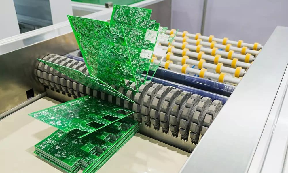
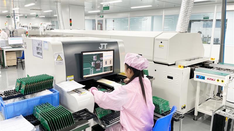
The PCB prototype production process for a PCB (Printed Circuit Board) manufacturer involves several key steps to create a working prototype of a printed circuit board before mass production. Developing a prototype allows designers and engineers to validate the design, test functionality, and identify and address any issues or improvements before moving to full-scale production. Below is an overview of the typical PCB prototype production process:

1. Design and Schematic Capture:
The process begins with the creation of a PCB design using specialized PCB design software. Designers create a schematic diagram of the circuit, defining the components and their connections.
Using the schematic as a reference, the PCB layout is designed. This involves placing the components on the PCB, routing traces (conducting pathways) to connect them, and defining the board's dimensions and shape.
3. Design Verification:
Before moving forward, the PCB design is thoroughly verified through design rule checks (DRCs) and electrical rule checks (ERCs) to ensure that there are no errors or violations of design constraints.
4. Gerber File Generation:
Once the design is verified, Gerber files are generated. Gerber files contain the information needed for manufacturing, including layer artwork, copper traces, component placement data, and drill hole positions.
5.Prototype Fabrication:
The manufacturer uses the Gerber files to fabricate the prototype PCB. This involves the following steps:
Substrate Selection:
Choosing the appropriate PCB substrate material, typically fiberglass or epoxy, and determining the number of PCB layers (e.g., single-sided, double-sided, or multi-layer).
Copper Cladding:
Applying a layer of copper to the substrate, which will be etched to create the conductive traces.
Photoresist Application:
Applying a layer of photoresist material to protect certain areas of copper from etching.
Exposure and Development: Using UV light to expose the PCB to the Gerber files' image, and then developing the exposed areas to reveal the copper traces' patterns.
Etching:
Immersing the PCB in an etchant solution to remove excess copper, leaving only the desired traces.
Drilling:
Precision drilling of holes for component mounting and vias (connections between layers).
Solder Mask Application:
Applying a solder mask to cover all areas except solder pads and vias.
Silkscreen Printing:
Adding component labels, reference designators, and other markings on the PCB surface.
Surface Finish:
Applying a surface finish (e.g., HASL, ENIG, or OSP) to protect the copper traces and ensure solderability.
6.Component Procurement:
Components required for the prototype are procured from trusted suppliers. These components should match the specifications outlined in the PCB design.
7. Assembly and Soldering:
Soldering the components onto the PCB is a critical step. This can be done manually or through automated surface mount technology (SMT) or through-hole technology (THT) assembly processes.
8.Quality Control and Inspection:
Thorough quality control and inspection processes are performed to ensure that the PCB prototype meets design specifications and industry standards. This includes checks for soldering quality, component placement accuracy, and electrical continuity.
9.Testing and Debugging:
The assembled PCB prototype is subjected to functional testing and debugging to verify that it operates correctly and meets the intended functionality. Any issues are identified and resolved.

10.Documentation and Reporting:
Detailed documentation, including test reports and any necessary design modifications, is generated during the prototype production process. This documentation is valuable for future reference and for scaling up to mass production.
11.Prototype Evaluation:
The prototype is evaluated by design engineers and stakeholders to ensure that it meets the design requirements and performance expectations. Any necessary design modifications or improvements are documented.
12. Iterative Process (if needed):
If the prototype reveals design flaws or areas for improvement, the design may need to be modified, and the prototype production process may be repeated until the desired functionality and quality are achieved.
Once the PCB prototype production process is complete, and the prototype meets all specifications and passes testing, it can serve as the basis for full-scale production. This process allows manufacturers and designers to refine their designs and ensure that the final product will be reliable and meet the intended purpose.
Address of Plant
PCB Factory:
A1 Building, B Zone, Ditang Industrial Zone, Ditang Road, Shajing Street, Bao'an District, Shenzhen, China
PCBA Factory:
Room 805, Room 806, Room 809, No. 96, Chuangqiang Road, Ningxi Street, Zengcheng District, Guangzhou City, Guangdong Province, P.R. China
Office Address:
Room 805, Room 806, Room 809, No. 96, Chuangqiang Road, Ningxi Street, Zengcheng District, Guangzhou City, Guangdong Province, P.R. China