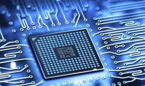
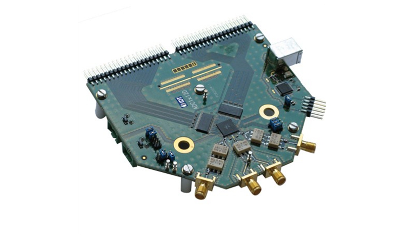
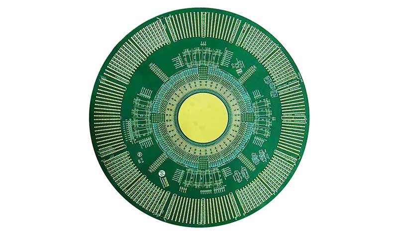
With the miniaturization of electronic devices, the use of thin PCB boards and small components is becoming popular. However, the use of thin multilayer PCBs with small SMT components also poses some problems. Often, such PCBs are subject to warpage during PCB assembly, which can affect their yield.
Let's take a quick look at what warpage really means before we find a solution that can help control it.

Normally, all parts of a printed circuit board should be in contact with the surface. However, sometimes this doesn't happen due to various stresses. What we have is a situation where some parts of the PCB bend upwards and some bend downwards resulting in positive and negative curvature. Sometimes the bend may be along the axis of the board or along the diagonal. The board can also sometimes appear to be twisted. All these are examples of PCB warpage.

Built-in stress on the copper film can cause board warpage. This is possible even at room temperature without any heat treatment.
In processes involving temperature variations, warpage can result due to the difference between the coefficient of thermal expansion between the copper layer and the substrate.
When individually etched copper clad panels are stacked together, the difference in copper density of each layer can result in different amounts of stress on each layer, which can lead to warpage.
PCBs are often placed in panels to improve PCB assembly efficiency. The legs are removed and the PCBs are separated by de-paneling. The difference in copper density between the circuit board area and the leg area further causes warpage.

In the case of PCB warpage, some parts of the PCB become closer to the template and some parts are further away. In turn, this causes solder paste deposits on the closer parts of the PCB to have a lower height. Deposits on parts with larger gaps have a higher height. Many problems can be seen with this uneven solder paste deposition.
It increases warpage when the temperature rises, for example during reflow. In turn, it can affect soldering under small pitch ICs.
Copper balancing - During the design phase itself, care must be taken to balance the copper in all layers. This helps to minimize mismatch in terms of coefficient of thermal expansion at room temperature as well as at elevated temperatures.
Balancing substrates between PCB layers - In multi-layer PCBs, care must be taken to use substrates with different CTEs.
Balancing copper density - During panelization, differences in copper density in the rail and leg areas of the panel need to be minimized.
Tray design- It is recommended to minimize the temperature difference between the PCB and the tray. The gap between the PCB edge and the tray edge also needs to be kept to a minimum.
Pre-treatment - Baking the PCB to above its Tg works well. This helps to soften the laminate while relieving the stress on the different layers. Thus, warpage is minimized.
It is important to work with a PCB contract manufacturer who has a thorough understanding of the various issues that can lead to PCB warpage. The above tips can go a long way in ensuring that warpage is kept at an acceptable level.
If you would like to learn more, about our technology, about the services we can provide, or a quote for a product, please contact us.
Address of Plant
PCB Factory:
A1 Building, B Zone, Ditang Industrial Zone, Ditang Road, Shajing Street, Bao'an District, Shenzhen, China
PCBA Factory:
Room 805, Room 806, Room 809, No. 96, Chuangqiang Road, Ningxi Street, Zengcheng District, Guangzhou City, Guangdong Province, P.R. China
Office Address:
Room 805, Room 806, Room 809, No. 96, Chuangqiang Road, Ningxi Street, Zengcheng District, Guangzhou City, Guangdong Province, P.R. China