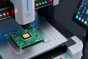
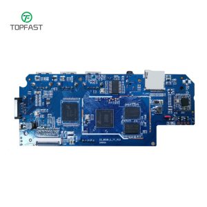
Em áreas exigentes como as comunicações de alta velocidade, o controlo industrial e a eletrónica de consumo topo de gama, a PCB de 10 camadas com orifício de passagem mantém uma posição insubstituível devido à sua fiabilidade excecional, forte capacidade de carga e processo de fabrico maduro. Diferente de IDH Os PCB de furo passante utilizam furos que penetram em todas as camadas para ligações eléctricas, proporcionando uma base física sólida para sistemas complexos.
Índice
Núcleo técnico das placas de circuito impresso com orifício passante de 10 camadas
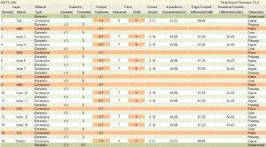
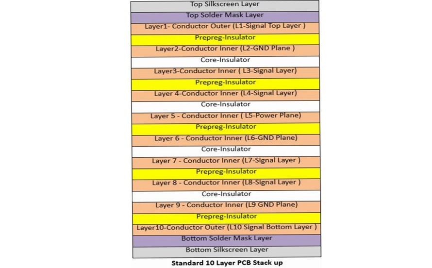
A essência da conceção de um PCB de 10 camadas com orifício de passagem reside na obtenção de um ótimo desempenho elétrico e resistência mecânica através de uma estrutura de empilhamento precisa. Uma pilha de camadas optimizada não só controla eficazmente a impedância, como também melhora significativamente a integridade do sinal e a compatibilidade electromagnética (CEM).
Uma estrutura típica de empilhamento recomendada é a seguinte:
| Ordem das camadas | Tipo de camada | Descrição da função principal |
|---|---|---|
| 1 | Camada de sinal | Camada superior, para colocação de componentes críticos e linhas de sinal de alta velocidade. |
| 2 | Plano de terra | Fornece um caminho de retorno completo para os sinais de topo e da camada 3, protegendo as interferências. |
| 3 | Camada de sinal | Forma um par "microstrip/stripline" com a camada 1 para uma qualidade de sinal óptima. |
| 4 | Camada de sinal | Encaminhamento de sinal interno. |
| 5 | Plano de potência | Fornece uma fonte de alimentação estável e de baixo ruído aos chips. |
| 6 | Plano de terra | Separa as ligações à terra digitais/analógicas, fornece referência para o plano de potência do núcleo. |
| 7 | Camada de sinal | Encaminhamento de sinal interno. |
| 8 | Camada de sinal | Forma um par "microstrip/stripline" com a camada 10. |
| 9 | Plano de terra | Fornece um plano de referência para os sinais da camada inferior. |
| 10 | Camada de sinal | Camada inferior, para a colocação de componentes e a saída de sinal. |
Pontos-chave do design:
- Controlo de impedância: Calcule rigorosamente a largura do traço, a espessura do dielétrico e a constante dieléctrica para garantir a continuidade de impedâncias críticas, como pares diferenciais (por exemplo, 100Ω).
- Via Design: Recomenda-se um diâmetro do orifício ≥ 0,2 mm e o diâmetro da almofada deve ser pelo menos 1,5 vezes o diâmetro do orifício para garantir uma boa estabilidade mecânica e ligação eléctrica.
Melhorar a estabilidade da transmissão de sinais
A estabilidade da transmissão do sinal é a chave para o sucesso de um PCB de 10 camadas com orifício de passagem. Isto baseia-se na seleção correta do material e em técnicas de processamento avançadas.
- Seleção do substrato: Para aplicações de alta velocidade ou de alta frequência, os laminados com baixa constante dieléctrica (Dk) e baixo fator de dissipação (Df) são recomendados, tais como Rogers RO4350B (Dk=3,48, Df=0,0037). Em comparação com o FR-4 normal, pode reduzir várias vezes a atenuação do sinal.
- Tipo de folha de cobre: Para reduzir as perdas por "efeito de pele" a altas frequências, devem ser selecionadas folhas de cobre com menor rugosidade superficial, tais como Folha de cobre recozida laminada (RACF) ou Folha de cobre de perfil muito baixo (HVLP).
- Processos de precisão:
- Perfuração a laser: Atinge uma precisão de perfuração de ±5μm, assegurando paredes de orifício lisas e reduzindo a reflexão do sinal.
- Revestimento uniforme: Uniformidade da espessura do cobre nos orifícios controlada dentro de ±2μm, assegurando uma transmissão de corrente consistente.
- Inspeção AOI e por raios X: Controlo de qualidade de todo o processo para eliminar potenciais defeitos.
2025 Custo aprofundado
Compreender a estrutura de custos da PCBs de 10 camadas com orifício passante é essencial para a orçamentação dos projectos e o controlo dos custos. Os preços de mercado de 2025 apresentam caraterísticas diversas.
1. Gama de preços de base:
- Material FR-4 padrão: Aproximadamente 500 - 2.000 RMB/metro quadrado.
- Lote pequeno/Protótipo: Os protótipos expedidos podem atingir 12,05 RMB por peça.
- Materiais de alta frequência/especiais: Como os laminados Rogers, que custam entre 2.000 e 5.000 RMB/metro quadrado.
2. Quadro de repartição dos custos principais:
| Categoria de custos | Proporção | Principais factores de influência e flutuações de custos |
|---|---|---|
| Materiais diretos | 40%-60% | - Substrato FR-4: 0,3-0,8 RMB/cm² - Material de alta frequência: 2-5 RMB/cm² - Folha de cobre: 3 oz é ~80% mais caro do que 1 oz |
| Taxas de processamento | 30%-45% | - O custo da perfuração a laser é 2-3 vezes superior ao da perfuração mecânica - O consumo de energia da laminação multi-prensa de 10 camadas é ~50% superior ao de 6 camadas - Cego/enterrado através do processo acrescenta o custo 30%-80% |
| Acabamento da superfície | 5%-10% | ENIG > HASL sem chumbo > OSP (O custo aumenta da esquerda para a direita) |
| Volume de encomendas | Impacto significativo | O custo dos lotes >50 ㎡ pode ser 40%-60% inferior ao dos protótipos |
3. Estratégias de redução de custos:
- Otimização da conceção: Relaxar a largura do traço para ≥ 4mil e o diâmetro do furo para ≥ 0,2 mm pode reduzir a dificuldade de processamento e o custo em 15%-25%.
- Compras a granel: Contactar diretamente as fábricas em regiões como Jiangxi ou Dongguan para a produção de grandes volumes, o que oferece vantagens significativas em termos de preços.
Processamento de tempos de espera e estratégias de aceleração Síntese
Estimar com exatidão o ciclo de produção para PCBs de 10 camadas com orifício passante é crucial para o planeamento do projeto.
- Prazo de entrega padrão:
- Prototipagem: 7-10 dias úteis.
- Produção em massa: 10-15 dias úteis.
- Principais factores de influência:
- Complexidade da conceção: Os requisitos especiais, como vias cegas/enterradas e controlo de impedância, podem acrescentar 3-5 dias.
- Volume de encomendas: Pequenos lotes (<10 ㎡) podem ser concluídos em 3-5 dias por lojas de produção rápida; volumes maiores requerem uma programação mais longa.
- Estratégias para reduzir o tempo de execução:
- Serviços Expeditos: Alguns fabricantes de Shenzhen (por exemplo, Junjiexin) oferecem Protótipo expedito 24 horas por dia mas custa 2 a 3 vezes mais do que o preço normal.
- Otimização de processos e fluxos: A utilização de Laser Diret Imaging (LDI), a otimização do design do painel e a seleção de fornecedores com equipamento avançado (por exemplo, os fornecedores de Shenzhen são frequentemente 1-2 dias mais rápidos) podem reduzir o ciclo total para 5-7 dias.
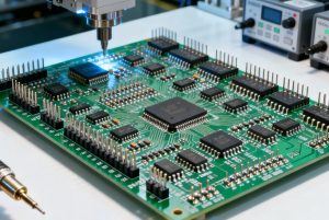
Como escolher uma qualidade Fabricante de PCB?
A escolha do fabricante certo é fundamental para o sucesso do projeto. Eis as principais dimensões para avaliar os fornecedores:
1. Avaliação da capacidade técnica:
- Nível do equipamento: Estão disponíveis máquinas de perfuração a laser de alta precisão, sistemas de exposição LDI, etc.?
- Experiência de processo: Têm experiência de produção em massa com placas de 10 camadas, especialmente no que diz respeito ao controlo da impedância e a capacidades fiáveis de revestimento?
2. Certificação do sistema de qualidade:
- Deve ter IPC-6012 (Qualification and Performance Specification for Rigid PCBs) e ISO 9001 certificações.
- Para os sectores automóvel/militar, verificar certificações como IATF 16949.
3. Lista de verificação da seleção de fornecedores:
| Dimensão da avaliação | Ação preferida | Prevenção de riscos |
|---|---|---|
| Localização geográfica | Preferir clusters industriais de PCB para uma resposta rápida da cadeia de abastecimento. | Evitar comerciantes sem fábricas físicas. |
| Estudos de casos de clientes | Solicitar histórias de sucesso em domínios relevantes (por exemplo, estações de base, controlo industrial). | Desconfie dos vendedores que não podem apresentar provas. |
| Apoio técnico | Confirmar a disponibilidade de serviços de valor acrescentado, como a revisão do DFM e o cálculo da impedância. | Rejeitar modelos OEM puros sem assistência técnica. |
Recomendação: Antes da decisão final, produzir 5-10 placas de teste para verificar aspectos fundamentais como a espessura do cobre nos orifícios (≥25μm) e o registo camada a camada, e clarificar os termos da reclamação de qualidade no contrato.
Cenários de aplicação e tendências futuras
PCBs de 10 camadas com orifício passante desempenham um papel fundamental nas seguintes áreas, devido à sua estabilidade superior e capacidade de interligação de alta densidade:
- Sistemas de controlo industrial: Exigem uma fiabilidade mecânica e térmica extremamente elevada para ambientes agressivos.
- Equipamento de comunicação da estação de base: Lidar com sinais complexos e transmissão de alta frequência, exigindo uma excelente integridade do sinal.
- Eletrónica de consumo topo de gama: Por exemplo, servidores, placas gráficas topo de gama, que necessitam de equilibrar o desempenho, o custo e a gestão térmica.
Com os avanços na ciência dos materiais e nos processos de fabrico, PCBs de 10 camadas com orifício passante estão a evoluir para frequências mais elevadas, maior densidade de potência e melhor desempenho de gestão térmica, continuando a fornecer uma plataforma de hardware sólida para dispositivos electrónicos da próxima geração.