Kopparplätering är en kritiskt steg som förvandlar borrade hål till tillförlitliga elektriska anslutningar.
Oavsett hur väl ett mönsterkort är utformat kan dålig kopparplätering leda till..:
- Intermittenta anslutningar
- Via sprickbildning
- För tidigt produktfel
Ur en tillverkares perspektiv är kopparplätering inte bara en kemisk process - det är en tillförlitlig gate.
Den här artikeln förklarar hur kopparplätering fungerar vid tillverkning av mönsterkort, de olika pläteringsstegen och hur tillverkare som TOPFAST kontrollera pläteringskvaliteten för att säkerställa långsiktig prestanda.
Innehållsförteckning
Vad är kopparplätering vid tillverkning av mönsterkort?
Kopparplätering är en process för att deponering av koppar på PCB-ytor och inuti borrade hål för att skapa elektriska anslutningar mellan lagren.
Plätering har två huvudsyften:
- Möjliggör elektrisk kontinuitet genom vias
- Uppnå den koppartjocklek som krävs för strömstyrka och tillförlitlighet
Typer av kopparplätering vid tillverkning av mönsterkort
Elektrolös kopparplätering
Elektrolös kopparplätering avger en tunt, enhetligt kopparskikt utan att använda elektrisk ström.
Syfte
- Skapa ett första ledande skikt inuti borrade hål
- Förbered kretskortet för elektroplätering
Typisk tjocklek:
- ~1-3 mikrometer
Detta steg är viktigt för att viorna ska bli elektriskt funktionella.
Elektrolytisk kopparplätering
Vid elektroplätering används elektrisk ström för att bygga upp koppartjockleken.
Syfte
- Förstärkning via väggar
- Öka koppartjockleken på ytan
- Uppfyller specifikationer för koppar i konstruktionen
Elektroplätering avgör:
- Via tillförlitlighet
- Strömförande kapacitet
- Mekanisk styrka
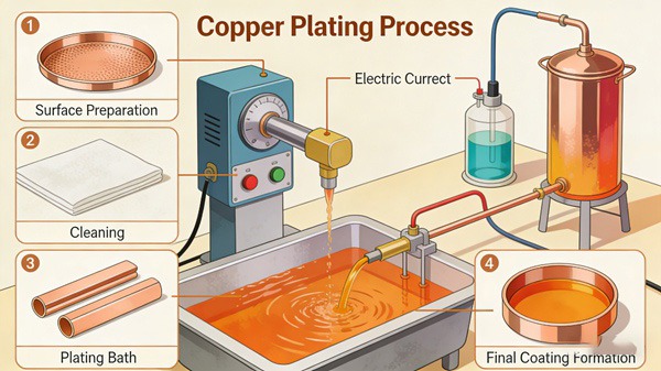
Steg-för-steg-process för kopparplätering
Steg 1 - Förberedelse av hålvägg
Efter borrning måste hålväggarna vara:
- Rengjord
- Avsmält
- Aktiverad för koppardeponering
Dålig förberedelse leder till svag vidhäftning av koppar.
Steg 2 - Elektrolös kopparbeläggning
Ett tunt kopparskikt deponeras på kemisk väg, vilket säkerställer:
- Enhetlig täckning
- Elektrisk kontinuitet
Detta skikt utgör grunden för all efterföljande plätering.
Steg 3 - Uppbyggnad av galvaniseringstjocklek
Koppartjockleken ökas genom kontrollerad elektroplätering.
Viktiga parametrar inkluderar:
- Aktuell densitet
- Badkemi
- Temperatur
- Pläteringstid
Konsekvens här är avgörande för tillförlitligheten.
Pläteringstjocklek och varför den är viktig
Via väggtjocklek
Via tillförlitlighet beror i hög grad på:
- Minsta koppartjocklek
- Enhetlig fördelning
Otillräckligt med koppar kan orsaka detta:
- Sprickor under termisk cykling
- Öppna kretsar
Yta Koppartjocklek
Ytlig koppar påverkar:
- Kapacitet för spårström
- Etsning av prestanda
- Impedansreglering
Hos TOPFAST anpassas pläteringstjockleken noggrant till konstruktionskraven för att undvika över- eller underplätering.
Vanliga defekter vid kopparplätering
H3: Tunnplätering
Orsakad av:
- Otillräcklig pläteringstid
- Dålig strömfördelning
Detta resulterar i minskad tillförlitlighet.
Tomrumsbildning
Tomrum inuti vior kan uppstå på grund av:
- Dålig rengöring av hål
- Ofullständig elektrolös täckning
Tomrum är en stor tillförlitlighetsrisk.
Ojämn plätering
Ojämn fördelning av koppar leder till:
- Svaga väggar
- Variation i impedans
- Avkastningsförlust
Hur kopparplätering påverkar kretskortens tillförlitlighet
Kopparpläteringens kvalitet har en direkt inverkan:
- Prestanda vid termisk cykling
- Motståndskraft mot mekanisk stress
- Långsiktig elektrisk stabilitet
I applikationer med hög tillförlitlighet är pläteringskvaliteten ofta avgörande mer än styrelseutseende.
Konstruktionsfaktorer som påverkar pläteringskvaliteten
Ur ett tillverkningsperspektiv blir plätering mer utmanande när:
- Bildförhållandet är för högt
- Hålstorleken är för liten
- Kopparfördelningen är ojämn
- Kraftiga kopparkonstruktioner används
Tidig DFM-granskning hjälper till att identifiera pläteringsrisker före produktion.
Tillverkarens perspektiv: Hur TOPFAST kontrollerar pläteringskvaliteten
På TOPFAST säkerställs kvaliteten på kopparplätering genom:
- Kontrollerad hantering av kemiska bad
- Övervakning av tjocklek i realtid
- Regelbunden tvärsnittsanalys
- IPC-anpassade acceptansstandarder
- DFM-driven designåterkoppling
Fokus ligger på stabil avkastning och långsiktig tillförlitlighetoch inte bara uppfylla minimikraven.
Kostnadsöverväganden vid kopparplätering
Kostnaden för kopparplätering ökar med:
- Höga krav på koppar
- Vior med högt aspektförhållande
- Snäva toleranser för tjocklek
- Avancerade specifikationer för tillförlitlighet
Genom att optimera kraven på plätering kan man avsevärt minska kostnaderna för mönsterkort utan att kompromissa med prestandan.
Slutsats
Kopparplätering är en av de mest kritiska processerna vid tillverkning av mönsterkort.
Den förvandlar borrade hål till hållbara elektriska anslutningar och definierar kretskortets tillförlitlighet.
Genom att förstå hur kopparplätering fungerar och vad som påverkar dess kvalitet kan designers och inköpare fatta smartare beslut som balanserar kostnad, prestanda och tillförlitlighet.
Med kontrollerade processer och tillverkningsexpertis, TOPFAST säkerställer kopparpläteringskvalitet som stöder tillförlitlig PCB-prestanda under hela produktlivscykeln.
Relaterad läsning
Tillverkningsprocessen för mönsterkort förklaras steg för steg
Förklaring av innerskiktets tillverkning
Vanliga frågor om kopparplätering
A: Kopparplätering skapar elektriska anslutningar mellan mönsterkortsskikten och säkerställer tillräcklig koppartjocklek för tillförlitlighet.
A: Elektrolös plätering skapar ett första ledande skikt, medan elektrolytisk plätering bygger upp koppartjockleken med hjälp av elektrisk ström.
A: Via koppartjocklek beror på design- och tillförlitlighetskrav, men måste uppfylla IPC-standarder för långsiktig prestanda.
S: Hålrum orsakas vanligtvis av dålig hålrengöring eller ofullständig täckning med elektrolös koppar.
A: Korrekt kopparplätering förbättrar motståndskraften mot termisk stress, mekanisk utmattning och elektriska fel.