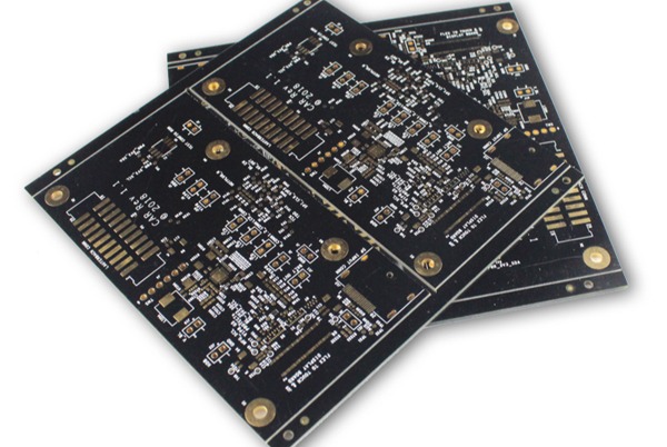
Tillverkning och kvalitetskontroll av flerskiktskretskort
I den digitala höghastighetsåldern har flerskiktskretskort blivit nyckeln till att förbättra prestandan hos elektroniska system. Antalet lager är dock inte nödvändigtvis detsamma som kvalitet. Ett mönsterkort med 6 lager av militär kvalitet kan vara mycket mer tillförlitligt än ett mönsterkort med 12 lager av konsumentkvalitet. Skillnaden ligger i den djupare logiken inom materialvetenskap, processtyrning och systemdesign.
Innehållsförteckning
Stapling av lager
- Grundläggande tillämpningar: Dubbelsidiga kort är tillräckligt för de flesta kraftmoduler (t.ex. LED-drivdon), där kopparvikten (1 oz vs. 2 oz) påverkar strömkapaciteten mer än antalet lager.
- Trösklar för prestanda: För signaler över 5 Gbps kan ett 4-lagers kort med optimerad stackup (t.ex. "signal-ground-power-signal") uppnå en överhörningsdämpning på -30 dB.
- Komplexa system: En 20-lagers växel kan använda "3-2-3" sammankopplingsstrukturer i alla lager för att uppnå 100 000+ via-densitet - här blir lagerantalet en verklig nödvändighet.
Antal lager ≠ kvalitet
1. Designkompatibilitet
Antalet lager måste motsvara kretsens komplexitet. Att öka antalet lager i blindo kommer att höja kostnaderna och medföra tillverkningsrisker.
2. Optimering av stackup-design
Felaktig lagerstapling kan orsaka signalreflektion och överhörning (t.ex. höghastighetssignaler som inte ligger i anslutning till jordlager).
3. Val av material
Högfrekventa tillämpningar kräver material med låg Dk/Df (t.ex. Rogers, Isola). Tjocka kopparkort kräver prepreg med hög hartshalt.
4. Processtyrning
Viktiga smärtpunkter: uppriktning mellan skikten (±75 μm), borrningsnoggrannhet (hålets grovhet ≤25 μm), hål i lamineringen (röntgeninspektion).
5. Testning och verifiering
100% elektrisk provning (flygande prob/AOI), impedansprovning (±10% tolerans) och CAF tillförlitlighetsprovning.
KRETSKORT Val av material
- Högfrekventa material Över 1 GHz orsakar standard FR4:s dissipationsfaktor (Df > 0,02) allvarliga signalförluster, vilket kräver högfrekventa material som Rogers RO4350B (Df = 0,0037).
- Kopparfolie: RTF (Reverse-treated foil) minskar ytjämnheten från 3 μm till 0,3 μm, vilket minskar 28 Gbps signalinsättningsförlust med 40%.
- Dielektrisk: Ett satellitprojekt hade en impedansavvikelse på 15Ω på grund av en tolerans på ±10% för dielektrisk tjocklek (jämfört med kravet på ±3%), vilket ledde till kostsamma omarbetningar.
Viktiga processer i kvalitetskontroll
- Precision: LDI-laseravbildning ökade registreringsnoggrannheten för 6-lagers kort från ±50 μm till ±15 μm - vilket motsvarar att hitta ett sesamfrö på en fotbollsplan.
- Lamineringsprocess: Ett ECU-kort för fordonsindustrin ökade från 65% till 92% genom att lamineringens ramphastighet sänktes från 3°C/min till 1,5°C/min, vilket gjorde att hartset flöt jämnt.
- Precisionsinstrument: För 18-lagers kort med 0,1 mm borr begränsas verktygets livslängd till 500 hål innan grovheten försämras från 8 μm till 25 μm.
Kärnprocess
- Tryckbindningsprocess: Matchning av TG-värden, kontroll av hartsflöde (fyllningsmängd ≥ 80%).
- Teknologi för bakåtborrning: Stubblängd ≤ 6 mil, vilket förbättrar signalintegriteten vid höga hastigheter.
- Ytbehandling: Elektrolytisk guldplätering (ENIG) är överlägsen varmluftslödning (HASL) och lämpar sig för BGA:er med fin pitch.
Verifiering av tillförlitlighet
- Destruktiv tvärsnittsmätning: Validerar pläteringens enhetlighet (mål: 18-25 μm koppar i vias).
- 3D-röntgeninspektion: Detekterar 0,05 mm² mikrovias fyllningsintegritet.
- Påskyndat åldrande: 1.000 timmar vid 85°C/85% RH simulerar 5 års driftbelastning.
Trender inom branschen
- Högfrekventa material: PTFE-substrat (millimetervågsradar/satellitkommunikation).
- Nyckelfärdiga tjänster: Välj leverantörer med IPC-6012 klass 3-certifiering (t.ex. Jiali Creation).
4 Större utmaningar och lösningar för tillverkning av mönsterkort med högt antal lager (10+ lager)
| Utmaning | Lösning |
|---|---|
| Felinställning mellan skikten | LDI laseravbildning + positionering av fyra spår (Pin LAM) |
| Låg avkastning på inre skikt | Spårbreddskompensation + Högprecisionsetsning (underskärning ≤15 μm) |
| Delaminering/hålrum i lamineringen | Laminering med stegvis uppvärmning + vakuumpress |
| Borrbrott/borrsprickor | Specialiserade borrkronor (efterslipning ≤3 gånger) + Reservbräda med hög densitet |


Relaterade inlägg