PCB montajı (PCBA), bir bilgisayarın Çıplak PCB işlevsel bir elektronik karta dönüşürPCB üretimi, tüm PCB üretim iş akışının temelini oluşturan çıplak tahta üretim aşamasına odaklanır. Bu aşama şunları içerir bileşen yerleştirme, lehimleme ve titiz testler
Montaj kalitesi doğrudan etkiler:
- Elektriksel işlevsellik
- Ürün güvenilirliği
- Üretim verimi
At TOPFAST, montaj bir verim odaklı süreçpanoların işlevsel ve sağlam olmasını sağlamak.
PCB montajının fabrikasyon ile nasıl ilişkili olduğuna dair arka plan için bkz: PCB İmalatı vs PCB Montajı
İçindekiler
Yüzey Montaj Teknolojisi (SMT) Montaj
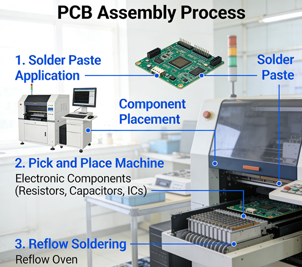
SMT Montajı Nedir?
SMT montajı montajı içerir yüzeye monte bileşenler kullanarak doğrudan PCB pedlerinin üzerine yerleştirin:
- Lehim pastası
- Alma ve yerleştirme makineleri
- Reflow lehimleme
SMT hızlı, hassas ve yüksek yoğunluklu levhalar için uygunTüketici elektroniği, telekomünikasyon ve IoT cihazlarında yaygın olarak kullanılır.
SMT Zorlukları
- İnce aralıklı bileşenler aşırı yerleştirme hassasiyeti gerektirir
- Yeniden akış sırasındaki termal stres, iç katmanlar veya bakır kaplama tutarsızsa PCB'lere zarar verebilir
- Yüksek yoğunluklu levhalar verim hassasiyetini artırır
TOPFAST'ta SMT montajı, üretim verileriyle dikkatli bir şekilde koordine edilerek kusurları en aza indirir ve verimi artırır.
Delikten Montaj
Delikten Montaj Nedir?
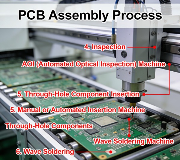
Delikten montaj, bileşenleri uçlarıyla birlikte delinmiş deliklere yerleştirir ve kullanarak lehimler:
- Dalga lehimleme (toplu lehimleme)
- Manuel lehimleme (prototipler veya düşük hacimli kartlar için)
Through-hole hala yaygın olarak kullanılmaktadır:
- Mekanik dayanım
- Yüksek güçlü bileşenler
- Konektörler ve büyük paketler
Delikten Montaj İş Akışı
- Delik Doldurma / Bileşen Yerleştirme - Bileşen uçlarını kaplamalı deliklere yerleştirin
- Lehimleme - Dalga veya seçici lehimleme bileşenleri sabitler
- Teftiş - Lehim kalitesi için görsel veya AOI kontrolleri
Delme ve kaplama kalitesi aşağıdakilerden doğrudan etkilenir PCB Delme vs Lazer Delmeve Bakır Kaplama Süreci Açıklandı.
Delik İçi Zorluklar
- Yanlış hizalanmış veya kötü kaplanmış delikler lehim bağlantı güvenilirliğini azaltır
- Manuel montaj işçilik maliyetini ve insan hatası potansiyelini artırır
- SMT'ye göre daha fazla pano alanı gerektirir
TOPFAST birleştirir montaj optimizasyonu ile hassas delme ve kaplama delik verimini en üst düzeye çıkarmak için.
Montajda Test ve Kalite Kontrol
Devre İçi Test (ICT)
ICT kontrolleri
- Şort
- Açılır
- Doğru bileşen değerleri
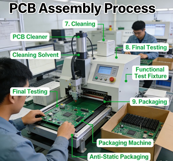
İşlevsel Test
İşlevsel test, kartın tasarlandığı gibi çalıştığını doğrulamak için gerçek dünyadaki çalışmayı simüle eder.
Test, imalat ve montaj adımlarının spesifikasyonları karşılamasını sağlayan son kontrol noktasıdır. Bkz. Aşındırma Süreci ve Verim Kontrolü Açıklandı erken aşama kalitesinin test sonuçlarını nasıl etkilediğine dair bir fikir verebilir.
Montaj Verimine İlişkin Hususlar
Verim
- İmalat kalitesi (örn. iç katmanlar, delme, kaplama)
- Bileşen yerleştirme doğruluğu
- Lehimleme parametreleri
- Kart tasarımı (termal, aralık, ped boyutu)
Yüksek verimli montaj azaltır:
- Rework
- Hurda
- Genel üretim maliyeti
- Bakınız PCB İmalatı vs PCB Montajı Verim hususlarının her iki süreci de nasıl kapsadığını görmek için.
Montajda Maliyet Faktörleri
Temel maliyet etkenleri:
- Bileşen tipi ve ambalajı
- Kart yoğunluğu ve katman sayısı
- Montaj hacmi (prototip vs seri üretim)
- Test ve denetim gereklilikleri
Kaliteden ödün vermeden montajı optimize etmek için tasarım, imalat ve montaj süreçleri arasında yakın uyum.
Sonuç
PCB montajı, çıplak bir kartı tamamen işlevsel bir elektronik ürüne dönüştürür.
SMT ve açık delik süreçlerisağlam testlerle birlikte nihai ürünün güvenilirliğini belirler.
İmalat kalitesi ile entegrasyonun sağlanması esastır:
- Yüksek verim
- Uygun maliyetli üretim
- Uzun vadeli güvenilirlik
PCB Montaj Süreci SSS
C: PCB montajı, elektronik bileşenlerin SMT veya açık delik teknikleri kullanılarak üretilmiş bir PCB üzerine monte edilmesini ve ardından inceleme ve test edilmesini içerir.
C: SMT, bileşenleri PCB'nin yüzeyine monte ederken, açık delik bileşen uçlarını delinmiş deliklere yerleştirir ve lehimler.
C: Yanlış hizalanmış katmanlar, kötü delinmiş delikler veya tutarsız kaplama lehimleme hatalarına neden olabilir ve montaj verimini düşürebilir.
C: Otomatik Optik Denetim (AOI), X-ray denetimi, Devre İçi Test (ICT) ve işlevsel test yaygın olarak kullanılmaktadır.
A: TOPFAST, imalat ve montaj süreçlerini hizalar, otomatik ve manuel denetimler uygular ve güvenilir üretim için verim odaklı optimizasyon kullanır