Amidst the surging trends of smart homes, smart cities, and Industry 4.0, IoT devices are quietly permeating every corner of our lives. PCBs have evolved beyond mere connection carriers to become the “skeletal system,” “neural network,” and “powerhouse” of IoT devices. This article delves into the inseparable relationship between PCBs and the Internet of Things, revealing how this small circuit board has become the invisible force propelling the era of universal connectivity.
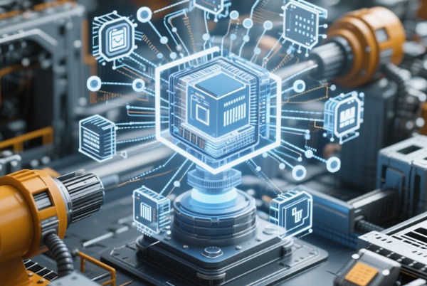
Table of Contents
The PCB: The “Multi-functional Integration Platform” for IoT Devices
The ability of IoT devices to sense, think, and communicate relies entirely on their internally coordinated electronic systems, with the PCB serving as the physical foundation.
The “Intelligent Traffic Network” for Signal Transmission
- The IoT data flow follows a “collection-conversion-decision-transmission” loop. The PCB builds a layered highway for this process:
- Sensing Layer: Connects sensors (e.g., temperature, motion). The PCB must provide stable analog signal paths and isolate noise through careful layout to ensure data accuracy.
- Processing Layer: Links the microcontroller and memory. High-speed digital signals travel across the PCB, where Signal Integrity design is crucial to prevent data distortion and errors.
- Communication Layer: Integrates wireless modules (Wi-Fi, Bluetooth, NB-IoT). This section acts as a miniature RF system, requiring precise impedance control and antenna design for stable signal transmission and reception.
The “Efficient Energy-Saving System” for Power Management
- Many IoT devices run on batteries for years. The secret to their ultra-long battery life lies in PCB power management design.
- Dynamic Power Control: Integrating Power Management ICs (PMICs) allows the system to intelligently shut down idle modules and reduce core voltage, slashing power consumption from milliamps to microamps.
- Precise Power Distribution: An optimized PCB layout minimizes current loss during transmission, like planning the shortest city routes for electricity to reach each component efficiently.
The “3D Innovation Space” for Structural Integration
- To fit the compact and irregular shapes of devices like smartwatches and doorbells, PCB technology continues to innovate in form factor.
- Rigid-Flex PCBs: Combine the stability of rigid boards with the flexibility of flex boards, allowing them to “bend” around components inside the device, maximizing space utilization.
- High-Density Interconnect (HDI): Utilizes microvias, blind vias, etc., to route thousands of connections in a thumbnail-sized area, achieving extreme functional integration.
Key PCB Technologies Addressing Core IoT Challenges
The specific demands of IoT directly drive the evolution of PCB technology, primarily seen in these four areas:
Miniaturization & High Integration: HDI and SiP Technologies
- HDI PCBs: Use microvia technology to enable finer lines and smaller pads, allowing components to be packed closely together. This is key for multi-functionality in small form factors like wearables.
- System-in-Package (SiP): An advanced technology that packages multiple chips (e.g., processor, memory) into a single unit. SiP drastically saves mainboard space and enhances system performance and reliability.
Low Power Consumption & Long Battery Life: Design and Material Optimization
- Power Integrity Design: Placing decoupling capacitor networks around key chips ensures stable voltage, preventing extra power drain from fluctuations.
- Low-Loss Materials: Using high-frequency, low-loss laminate materials for communication modules reduces energy loss during signal transmission, allowing data to be sent using less power.
Reliability & Environmental Ruggedness: Materials and Process Assurance
- Specialty Material Application: In harsh environments (industrial, automotive), PCBs use High Tg materials or metal-core substrates to withstand high temperatures, humidity, and corrosion.
- Protective Conformal Coating & Potting: Processes like conformal coating and potting put a “protective suit” on the PCB, making it resistant to moisture, mold, and chemicals.

Future Outlook: How Will PCBs Continue to Enable IoT Innovation?
As IoT evolves towards greater intelligence and edge computing, PCB technology will face new opportunities and challenges:
- AIoT Integration: Edge computing devices with built-in AI algorithms require PCBs to support higher computational density and faster signal processing.
- Sustainability: Eco-friendly materials and recyclable PCB manufacturing processes will become key industry topics.
- Cost-Performance Balance: In a competitive market, the ability to balance cost control without sacrificing performance through innovative design and manufacturing is a core competency for PCB suppliers.
Conclusion
In summary, the relationship between PCB and IoT is symbiotic and co-evolutionary. IoT demands chart the course for PCB technology advancement, while every breakthrough in PCB technology, in turn, unlocks new form factors and applications for IoT devices. This green board hidden inside our devices is the steadfast, reliable foundation silently supporting our connected world.