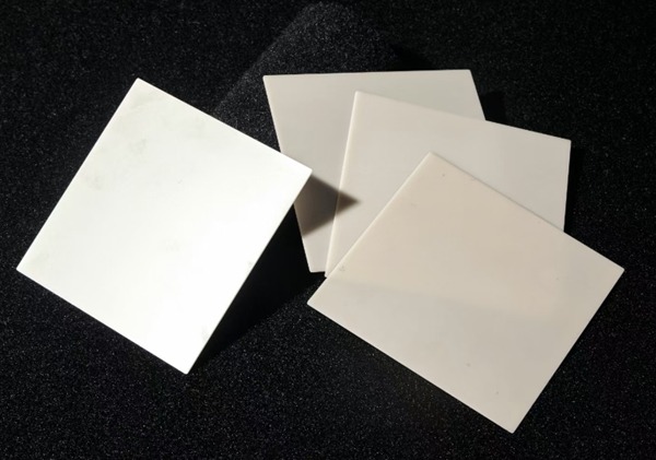
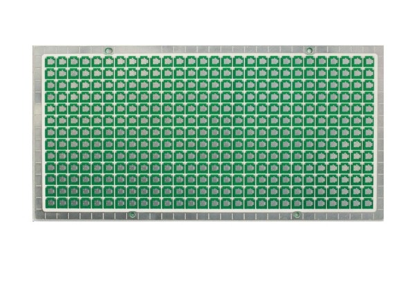
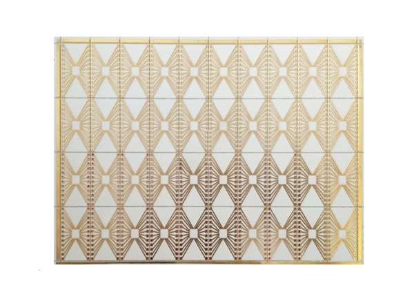
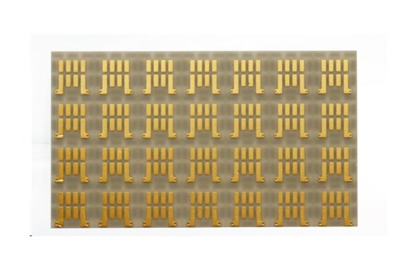
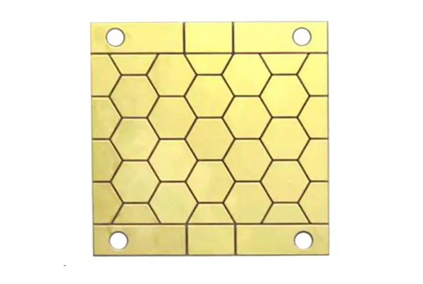
Thermal Stability · High Power · Extreme Environment

Ceramic
Printed Circuit
Boards

Superior thermal management with Alumina (Al2O3) and Aluminum Nitride (AlN) substrates for high-power, high-frequency, and aerospace applications.

Ceramic PCB
170W/m·KMax Conductivity
800°COperating Temp
Home /Ceramic PCB
IPC-A-600Acceptability of Printed Boards
High ThermalSuperior Dissipation
ISO 9001Quality Management
Ceramic BaseAlumina & AlN
UL 94V-0Flammability Rating
Low CTEDimensional Stability
Product Range

Ceramic PCB Technologies

Advanced ceramic substrates for the most demanding thermal and electrical requirements

Alumina (Al2O3) PCB
01

Alumina (Al2O3) PCB

The most cost-effective ceramic solution, offering excellent electrical insulation and mechanical strength for general high-temperature applications.

  • 96% - 99% Alumina content
  • Thermal conductivity: 24-30 W/m·K
  • Excellent dielectric properties
Request Quote
Aluminum Nitride (AlN) PCB
02

Aluminum Nitride (AlN)

Ultimate thermal management with conductivity up to 170 W/m·K, ideal for high-power LED and power semiconductors.

  • Extreme thermal dissipation
  • CTE matching Silicon
Request Quote
DBC / DPC Technology
03

DPC & DBC Process

Direct Plated Copper (DPC) for high-precision circuits and Direct Bonded Copper (DBC) for high-current power modules.

  • Ultra-fine trace capability
  • Thick copper bonding
Request Quote
Multilayer Ceramic PCB
04

HTCC & LTCC

High/Low Temperature Co-fired Ceramics for complex multilayer ceramic structures with integrated passive components.

  • Multilayer integration
  • Superior hermeticity
  • High-frequency stability
Request Quote
Capabilities

Technical Specifications

Our ceramic PCB manufacturing parameters at a glance

24–170W/m·K
Thermal Conductivity
Alumina to AlN
±0.02mm
Laser Accuracy
Precision via drilling
0.25–2.0mm
Substrate Thickness
Standard ceramic sheets
4–7ppm/°C
CTE
Close to Silicon chip
>20KV/mm
Breakdown Voltage
Excellent insulation
Gold/Silver
Surface Finish
ENIG, ENEPIG, Plated Au
Substrates

Ceramic PCB Materials

Compare our ceramic cores for different thermal and frequency requirements

Property FR-4Standard Alumina96% Al2O3 AlNAluminum Nitride Silicon CarbideSiC
Thermal Conductivity 0.25 W/m·K 24 – 30 W/m·K 150 – 170 W/m·K 200+ W/m·K
Dielectric Constant 4.2 – 4.6 9.0 – 10.0 8.5 – 9.0 ~40
Operating Temp Up to 170°C Up to 800°C Up to 800°C Up to 1000°C
CTE (Z-axis) 50-70 ppm 6-8 ppm 4-5 ppm 3.7 ppm
Durability
Cost Level

● Green = performance level  ·  Amber = relative cost  ·  Ceramic substrates offer ultimate thermal stability for high-power modules.

Get Online Quote
How It's Made

Manufacturing Process

High-precision ceramic fabrication with state-of-the-art laser and plating tech

01

Substrate Sourcing

Selection of high-purity Alumina or Aluminum Nitride. Substrates undergo ultrasonic cleaning and surface treatment to ensure bonding quality.

Al2O3AlNCleaning
02

Laser Drilling & Scripting

Using CO2 or UV lasers to drill high-precision through-holes and scribe individual boards with micron-level accuracy.

Laser DrillMicron-Precision
03

Metallization (DPC/DBC)

Thin-film deposition (DPC) or high-temperature bonding (DBC) to create robust copper layers on the ceramic surface.

SputteringCu Bonding
04

Patterning & Plating

Fine-line circuit imaging followed by electroplating and high-end surface finishes like ENIG or Electrolytic Gold.

Fine TracePlated GoldFinal AOI
Catalog

Ceramic PCB Products

Custom ceramic PCB fabrication for high-power, medical, and aerospace applications

Power illumination PCB
CeramicAluminaHigh-Power

Power illumination PCB

Power Lighting PCBs are printed circuit boards (PCBs) used in power and lighting equipment

Deep Ultraviolet (DUV) purifier PCBs
CeramicAluminaHigh-Power

Deep Ultraviolet (DUV) purifier PCBs

Deep Ultraviolet (DUV) purifier PCBs are specialized circuit boards designed to power and control UV-C disinfection…

FAQ

  • What certifications do PCB factories have?

    All of our products are IPC rated with ISO 14001; ISO 9001; CE; ROHS certificates, etc. Our products are widely used in communication, medical equipment, industrial control, power supply, consumer electronics and aerospace, automotive industry and other fields.

  • How many layers is a Ceramic PCB?

    According to the different needs, different processes, our factory can do ceramic circuit boards, can do the traditional process layer 2-8 layers, using low temperature co-fired ceramic (LTCC) and high temperature co-fired ceramic (HTCC), can reach 10-20 layers, or even higher. In actual application we will choose according to the customer, the type of process required and demand.

  • Commonly used ceramic circuit board processes

    Using the common ceramic circuit board thick film process, it is an advanced printed circuit board manufacturing technology with the advantages of easy multi-layer wiring, low cost, high temperature resistance, corrosion resistance, good mechanical strength, etc., which is widely used in the fields of electronics, communications, aerospace and so on.

  • Is it possible to produce a ceramic PCB with only a picture and no Gerber file?

    We can't produce without gerber file, we produce based on Gerber. Or if you have any samples, we can also clone based on the samples, if so, we can send 3-5 samples to our company, and then evaluate the price of making samples for you.

  • What is your delivery time?

    The fastest delivery time we can support is 12 hours. 1 hour for prompt quotation. 4 hours for prompt engineering. This depends on your product requirements and quantity. In addition, lead time will be included in your quote.

  • Where are your circuit boards manufactured?

    As a global PCB manufacturer, our factories are located in Guangzhou, China and Shenzhen, China, utilizing the strengths of each region to best serve you.

Knowledge Hub

Ceramic Insights

Technical articles and industry trends on high-thermal PCB manufacturing

Ready to start?

Launch Your Ceramic PCB Project Today

Submit your designs for high-thermal Alumina or AlN boards. Our engineers provide expert DFM feedback for ceramic substrates.