Energy Equipment PCB Manufacturing
& Assembly Services
Robust, High-Voltage PCB Solutions for Solar Inverters, Wind Power Systems, Energy Storage (ESS) and EV Charging Infrastructure.
Why Choose Us for Energy Equipment PCB
We empower the global energy transition by delivering the industry's most robust heavy copper and high-voltage PCB solutions for clean power generation and storage.
Heavy Copper Mastery
Industry-leading capability of up to 12oz heavy copper circuits, enabling the handling of high currents required for inverters and chargers.
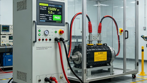
High-Voltage Safety
Expertise in 1000V–1500V DC layouts with rigorous creepage and clearance design to meet strict international safety standards.
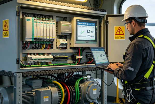
Advanced Thermal Management
Usage of Metal Core PCBs (MCPCB), ceramic substrates and embedded copper coins to dissipate extreme heat from power semiconductors.
ESS & BMS Expertise
Specialized fabrication for multi-cell battery management systems (BMS) with high-reliability data link and balanced power paths.
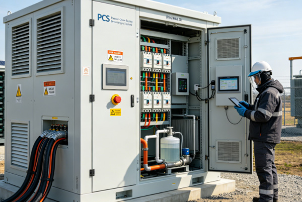
Rugged Environmental Protection
Durable board solutions designed for 20+ year lifespans in outdoor solar farms, wind parks and coastal charging installations.
System Integrity Mastery
Full support for power-integrity simulation and high-voltage testing to ensure zero failure in critical energy infrastructure.
Elite Engineering for High-Power Infrastructure
Our energy equipment specialists bridge the gap between massive current requirements and reliable hardware — providing PCB designs that ensure peak conversion efficiency and long-term grid stability.
Advanced simulation to ensure uniform current distribution and minimize resistive losses.
Strategic placement of thermal vias and metal cores to protect high-power MOSFETs and IGBTs.
Precision creepage, clearance and slot design for meeting IEC 62109 and UL 61010 standards.
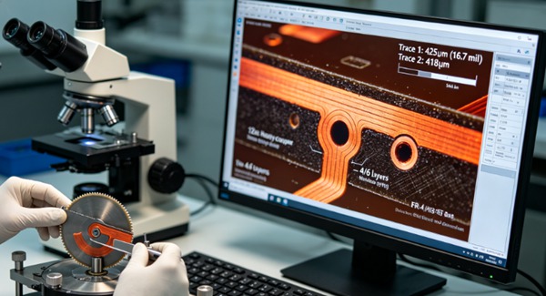
Ensuring layer-to-layer registration and etching precision on industry-leading copper thicknesses.
Energy Equipment PCB Capabilities
TopfastPCB delivers scalable PCB solutions for global clean energy expansion, from local residential solar inverters to massive grid-scale storage systems.
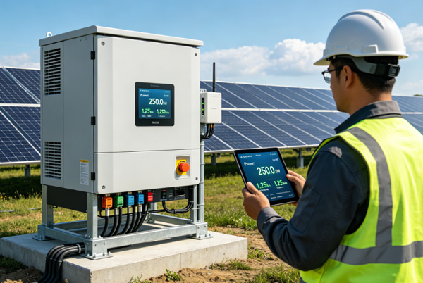
Solar conversion PCBs
Heavy copper solutions for high-efficiency PV inverters (up to 1500V DC) and power conversion units.
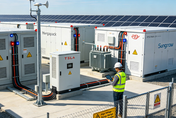
Energy Storage (ESS)
High-reliability PCBs for Battery Management Systems (BMS) and intelligent grid storage controllers.
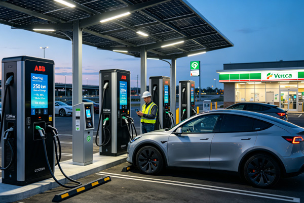
EV Charging Nodes
Rugged PCBs for DC fast chargers and residential level-2 charging stations with high thermal stability.
Heavy Power Execution Workflow
Engineering review focusing on copper weight, creeps and thermal dissipation.
Specialized etching and plating for extreme 12oz heavy copper circuits.
High-torque assembly for massive components and high-current connectors.
100% HI-POT and thermal stress testing for mission-critical grid reliability.
Energy Application Ecosystem
TopfastPCB powers the world's most innovative clean energy brands, providing scales of reliability across diverse power and storage categories.
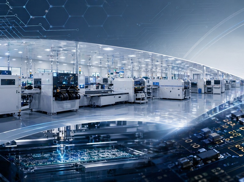
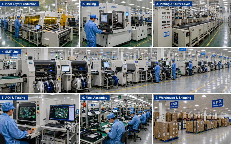
Heavy Power Innovation Center
Our world-class facility is optimized for the extreme currents and voltage of the energy sector, featuring specialized heavy copper etching lines and high-voltage HI-POT testing.
Chosen by the World's Clean Energy Leaders
Innovative solar equipment brands, wind power leaders and ESS technology innovators rely on TopfastPCB for their global power conversion hardware.


Energy Equipment FAQ
Common questions about high-power energy PCB technology, thermal management and safety standards.
Ask a Specialist →We leverage industry-leading fabrication technology to produce heavy copper PCBs with up to 12oz copper weight. This capability is essential for handling the extreme currents in utility-scale solar inverters and EV fast-charging stations.
For systems operating at 1000V–1500V DC, our engineers provide specialized DFM reviews focusing on creepage and clearance. We use high-precision routing and optimized slot design to ensure full compliance with IEC 62109 and UL safety standards.
We offer a range of advanced thermal solutions, including Metal Core PCBs (AL/CU), partial heavy copper, and embedded copper coin technology. These methods allow us to remove heat directly from power semiconductors, ensuring system efficiency and longevity.
Yes. For solar and wind applications, we use high-Tg materials and CAF-resistant substrates combined with specialized conformal coatings. Our manufacturing processes are designed to survive the thermal cycling and humidity of outdoor energy installations for decades.