Medical PCB Manufacturing
& Assembly Services
High Reliability Medical Grade PCB Solutions for Diagnostic Imaging, Patient Monitoring and Life Support Systems.
Why Choose Us for Medical PCB
From component sourcing to sterile-ready delivery, we are built for the strict demands of medical electronics — precision, safety, and full traceability.
ISO 13485 Certified
Full compliance with Quality Management Systems for medical devices, ensuring safety and efficacy in every board.
Miniaturization Mastery
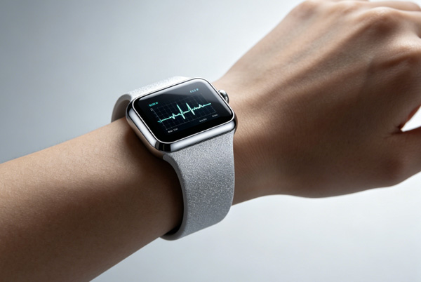
Advanced HDI and micro-miniaturization capabilities for compact wearables, handheld devices and diagnostic tools.
Full Traceability
Rigorous documentation and component traceability matching the strict compliance needs of medical device regulations.
Rapid Prototyping
Fast-track development cycles to help medical device manufacturers get to market quicker through iterative design testing.
Biosafe Materials
Expert selection of substrates and finishes that meet biocompatibility requirements and withstand sterilization processes.
Collaborative Support
Our medical PCB engineers offer DFM support, ensuring designs are optimized for mass production and clinical reliability.
Precision Engineering for Lifesaving Medical Technology
Our dedicated medical PCB engineers work closely with your team from R&D to production — optimizing PCB design for safety, signal integrity, and manufacturability in critical clinical applications.
Specialized design for manufacturing checks focusing on medical standards and miniaturization.
High-precision simulation for ultra-sensitive sensors and diagnostic imaging circuits.
Strategic heat management to ensure patient safety and comfort in body-worn electronics.
Validation of long-lifecycle medical components to prevent obsolescence in long-term device platforms.
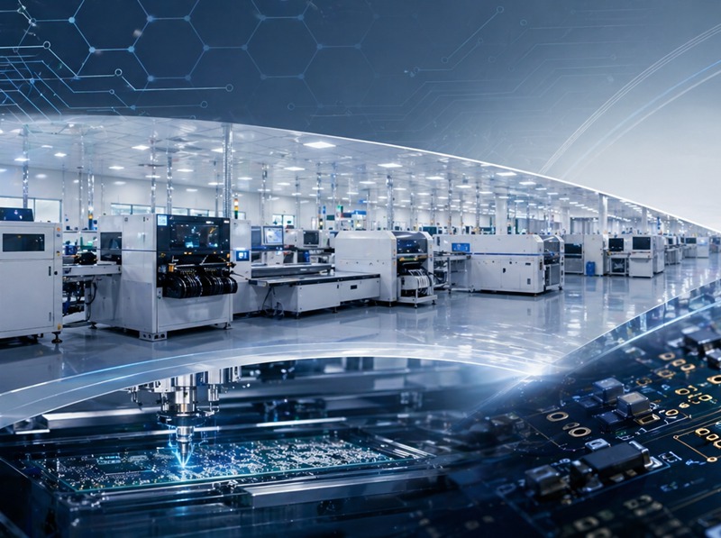
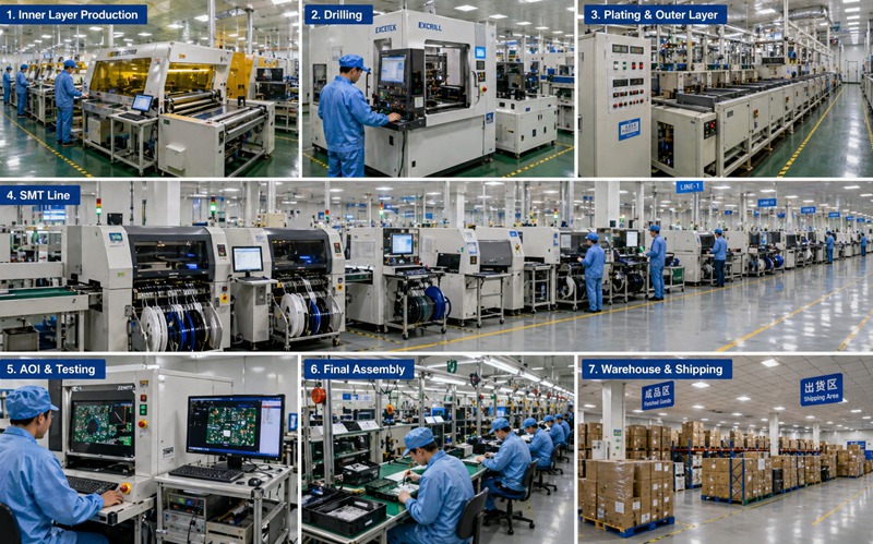
Medical PCB Manufacturing Capabilities
TopfastPCB provides high-reliability PCB fabrication and assembly for the healthcare industry, including mini-HDI for wearables, flexible circuits for surgical robotics and high-layer count boards for MRI systems.
Rigid Flex PCB
Space-saving interconnect solutions for ergonomic medical wearables and articulating surgical instruments.
HDI / Microvia
High-density interconnect technology enabling the miniaturization of diagnostic tools and portable patient monitors.
Biosafe / Ceramic
Use of specialized biocompatible substrates and ceramic cores for implantable devices and lab equipment.
Medical Manufacturing Workflow
Medical-grade engineering review and design validation.
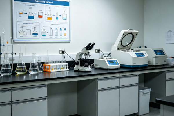
Precision multilayer fabrication in ISO-certified environment.
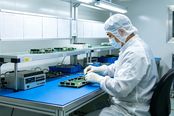
ESD-controlled assembly with full lead-free compliance.
AOI, X-ray and 100% functional testing for zero-failure delivery.
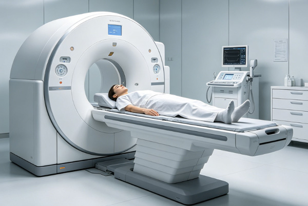
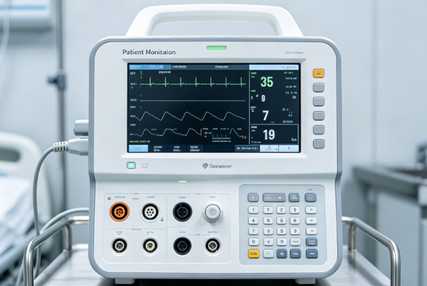
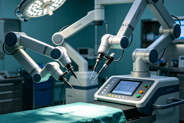
Medical PCB Applications
Trusted by medical device engineers worldwide for high-reliability PCB solutions across every life-critical medical application.
Medical Grade Manufacturing Excellence
Our ISO 13485 certified facility features ESD-controlled environments, high-precision laser drilling and automated inspection to provide zero-defect medical PCB solutions.

Chosen by Medical Tech Leaders Worldwide
Innovative healthcare companies and med-tech organizations rely on TopfastPCB for their mission-critical patient care projects.


Medical PCB FAQ
Common questions about medical grade PCB design, compliance and manufacturing.
Ask a Specialist →ISO 13485 is a quality management system specifically for medical devices. It ensures that the manufacturer follows strict guidelines for safety, traceability, and risk management throughout the PCB fabrication and assembly process.
We provide full component traceability, including batch numbers and dates of manufacture, recorded within our ERP system. We can provide full documentation packs to support your FDA or CE regulatory submissions.
Yes. We leverage advanced HDI features like any-layer microvias, 3/3 mil trace/space, and rigid-flex technology to enable the extreme miniaturization required for modern smart health wearables and diagnostic instruments.
Yes, we offer full lead-free assembly and materials that are fully RoHS and REACH compliant to meet international environmental and safety standards for medical device housing and circuitry.