What certifications do PCB factories have?
All of our products are IPC rated with ISO 14001; ISO 9001; CE; ROHS certificates, etc. Our products are widely used in communication, medical equipment, industrial control, power supply, consumer electronics and aerospace, automotive industry and other fields.
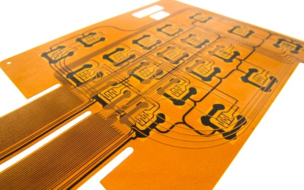
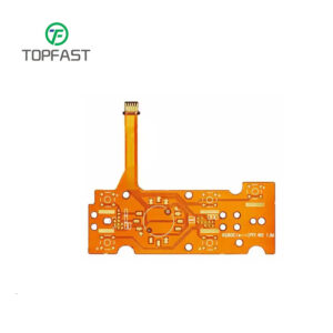
What types of flexible PCBs do you offer?
Topfast always adheres to the service concept of customer first and quality first, and provides diversified customized services, which can produce single-sided boards, double-sided boards, multilayer boards and so on.
What are the advantages of your flexible boards over other manufacturers?
The company has world-class production equipment (laser drilling machine, VCP through-hole filling line, blind hole AOI testing equipment, ceramic grinding line, vertical vacuum resin blocking machine, etc.), first-class technical team, mature product line, perfect service flow, to provide one-stop PCB services from design, sampling to mass production and assembly.
What is the lead time for PCB boards?
We can deliver double-sided samples in 24 hours at the earliest, but we need to evaluate the delivery time according to the design file and the quantity.
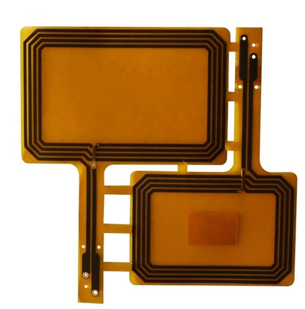
What are the main applications of flexible circuit boards?
The products are widely used in communication (cell phones, computers, etc.), medical equipment (blood analyzers, hearing aids, etc.), industrial control, power supply, consumer electronics and aerospace, automotive industry and other fields.
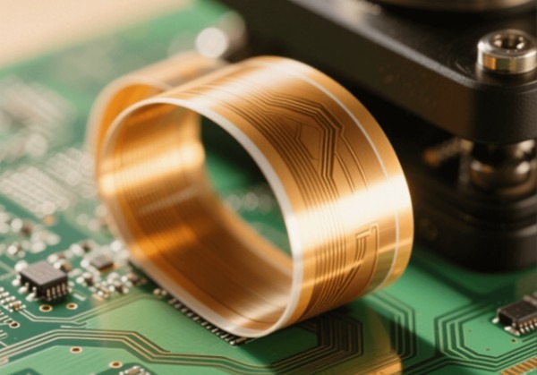
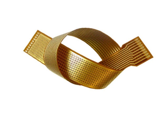
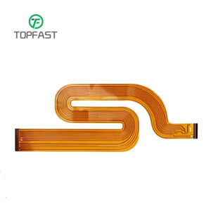
What materials are used in flexible PCBs?
Flexible PCBs typically use copper as the conductive layer and polyimide as the insulating material. In addition, adhesives and reinforcing ribs are used to bond and support the layers.
What is the typical thickness of a flexible PCB?
The typical thickness range for a 2-layer flexible PCB is 0.11 mm to 0.2 mm.
Can flexible PCBs be customized for specific applications?
Yes, flexible PCBs can be fully customized in terms of size, shape, layer count, and materials to meet the specific requirements of your application.
Can flexible PCBs withstand high temperatures?
Flexible PCBs are designed to withstand a wide range of temperatures, making them suitable for automotive, aerospace, and industrial applications where thermal management is critical.
 News
News