AI Smart Care PCB Manufacturing
& Assembly Services
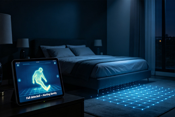
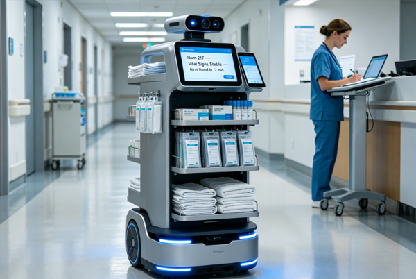
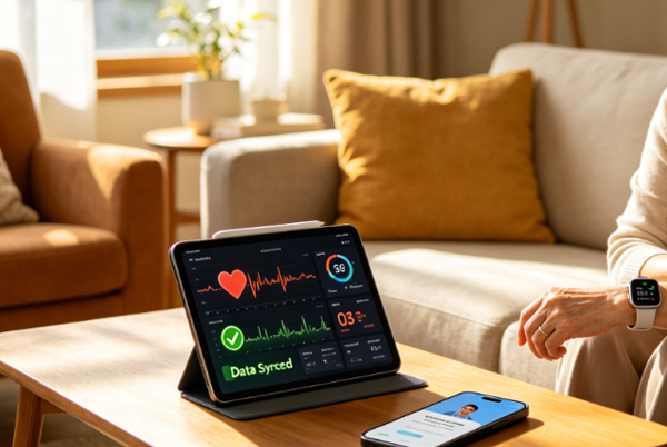
Intelligent PCB Solutions for AI Health Monitoring, Smart Nursing, Personal Safety and Remote Clinical Care Systems.
Why Choose Us for AI Smart Care PCB
We empower the next generation of intelligent care by delivering high-precision PCBs optimized for AI edge processing, sensor fusion and ultra-reliable connectivity.
Edge AI Hardware Support
Advanced fabrication supporting high-speed processing units (NPUs/TPUs) for real-time health data analysis at the device level.
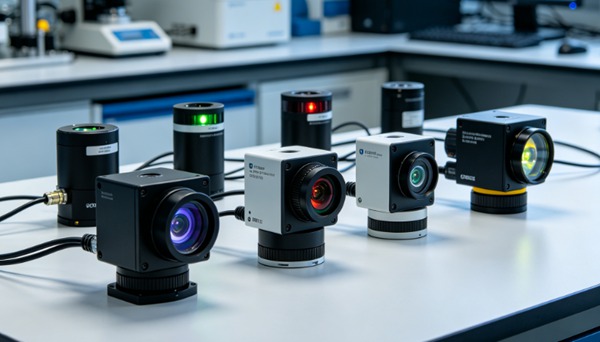
Multi-Sensor Integration
Expertise in multi-layer PCB design for sensor fusion, combining Lidar, IR thermal, voice and motion tracking on ultra-compact boards.
Clinical-Grade Quality
Full compliance with ISO 13485 (Medical) standards, ensuring that AI care devices meet the highest safety and reliability requirements.
Bio-Compatible Options
Selection of substrates and surface finishes that meet biocompatibility requirements for skin-contact AI wearables and monitoring patches.
High-Reliability IoT
Optimized RF engineering for seamless 5G, Wi-Fi 6 and Bluetooth connectivity in distributed smart nursing home environments.
Dedicated Innovation Team
Our engineers provide rapid prototyping and DFM support to hardware startups and healthcare tech giants developing AI care solutions.
Intelligent Engineering for Proactive Healthcare
Our smart care engineering team bridges the gap between complex AI algorithms and reliable hardware — providing PCB designs that ensure high-precision data capture and autonomous decision-making.
Designing for low-latency processing architectures and high-density chipsets.
Isolation techniques to protect high-sensitivity vital sign sensors from digital noise.
Strategic design to extend battery life for wearables in continuous monitoring mode.
Pre-compliance engineering to ensure hardware passes medical-grade EMI/EMC testing.
AI Smart Care PCB Capabilities
TopfastPCB delivers high-reliability PCB solutions for AI-integrated care technology, from non-invasive fall sensors to data-heavy smart nursing consoles.
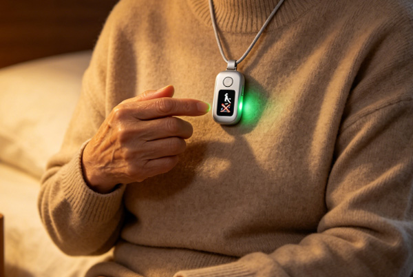
Rigid-Flex Care Wearables
Comfortable, ergonomic rigid-flex PCBs for 24/7 personal safety trackers and medical alert bands.
High-Density AI Processing
Multi-layer HDI technology optimized for fast AI data processing and intelligent medication control.
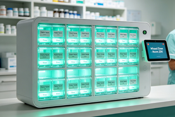
Smart Sensor Boards
Integration-ready PCBs for non-invasive radar, thermal imaging and acoustic elderly care sensing.
Solution Realization Workflow
DFM and engineering review focused on AI hardware compatibility.
Reliable fabrication using medical-grade environmental controls.
High-precision assembly for fine-pitch AI chips and multi-sensors.
Combined AOI, X-ray and RF testing for zero-failure field operation.
AI Smart Care Applications
TopfastPCB powers leading innovation in proactive elder care and intelligent nursing, providing scales of reliability across the entire smart care ecosystem.
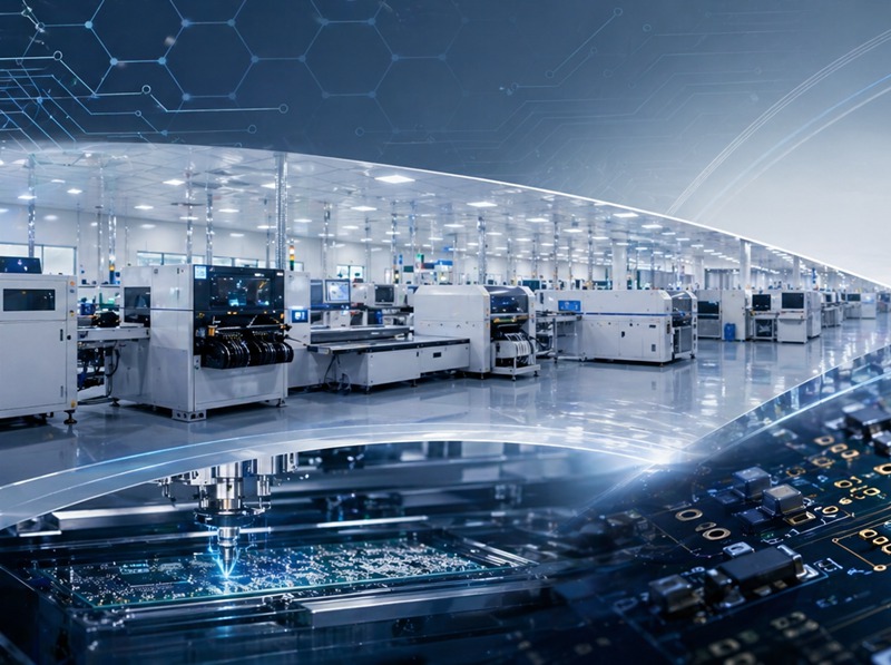
Medical-Grade Innovation Center
Our ISO 13485 certified facility is equipped for high-precision smart care electronics, featuring specialized SMT lines for AI hardware and sensor-rich assemblies.
Chosen by Smart Care Pioneers
Leading healthcare startups and established smart care organizations rely on TopfastPCB for their proactive life-safety hardware.


AI Smart Care FAQ
Expert answers about smart care PCB technology, sensor integration and medical compliance.
Ask a Specialist →We leverage advanced multi-layer HDI technology and high-Tg materials to support ultra-fine pitch BGA assemblies for NPUs and TPUs, ensuring the stable power delivery and high-speed data paths required for Edge AI processing.
Yes. Our engineering expertise includes routing high-sensitivity sensor signals (Radar, PIR, Thermal) with specialized isolation and shielding techniques to ensure cross-sensor interference is eliminated on small healthcare-grade boards.
While we are a manufacturer, we offer material validation documentation for our ENIG/ENEPIG finishes and flexible substrates that are commonly used in skin-contact applications, helping you meet medical-grade safety standards.
Our dedicated RF engineers provide antenna matching and layout services for multi-protocol environments (Mesh Wi-Fi, BLE, 5G), ensuring that distributed care sensors maintain a rock-solid connection even in complex building layouts.