Communication PCB Manufacturing
& Assembly Services
Advanced PCB Solutions for 5G Base Stations, High-Speed Data Center Switches, Enterprise Routers and Optical Infrastructure.
Why Choose Us for Communication PCB
We empower the global digital infrastructure by delivering edge-to-core PCB solutions optimized for 28Gbps+ signaling, extreme thermal loads and high-density backplanes.
High-Speed Digital (HSD) Mastery
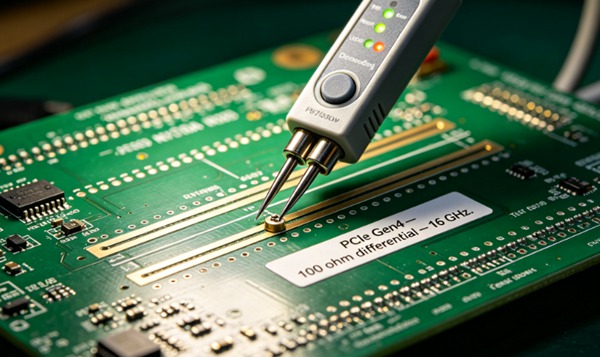
Advanced fabrication for 25Gbps, 28Gbps and upcoming 56Gbps signaling paths with sub-5% impedance tolerance.
Ultra-Low Loss Interconnects
Strategic use of Low-Dk/Low-Df materials such as Megtron 6/7 and Rogers to minimize signal attenuation in 5G infrastructure.
Advanced Backplane Capacity
Manufacturing ultra-thick, high-layer count backplanes (30+ layers) with precision press-fit and high-density connectors.
Signal stub Elimination
In-house precision back-drilling capability to remove signal stubs and maintain flawless eye-diagram patterns for network switches.
Massive Thermal Solutions
Integrated thermal coins and heavy copper layers for power-hungry 5G Massive MIMO antennas and data center processors.
Network Logic Reliability
Full support for telecom-grade reliability testing, ensuring 24/7 uptime for mission-critical core network infrastructure.

Elite Engineering for Global Connectivity
Our communication engineering specialists bridge the gap between high-frequency physics and reliable hardware — providing PCB designs that ensure maximum network bandwidth and zero signal crosstalk.
Simulation-driven layout optimization for 28Gbps/56Gbps differential pair routing.
Advanced heat dissipation analysis for massive MIMO antenna systems and RRU modules.
Strategic hybrid material selection for balancing cost and high-frequency performance.
Rigorous manufacturing reviews for ultra-thick, high-layer count communication backplanes.
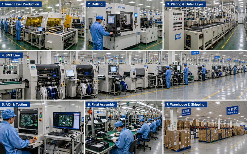
Communication PCB Manufacturing Capabilities
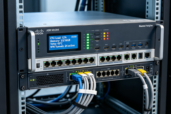
TopfastPCB delivers scalable PCB solutions for global network infrastructure, from local wireless access nodes to core high-speed data center switching.
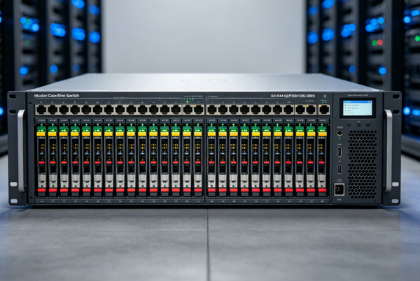
Network Switch HSD
Precision multi-layer PCBs optimized for ultra-high speed network switching and data center routing.
5G Massive MIMO
Advanced RF boards with integrated thermal solutions for 5G active antenna units and base station RRUs.
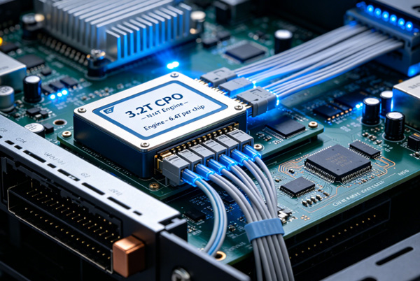
Optical Interface
High-precision PCBs for optical transceivers and fiber infrastructure equipment supporting OTN networks.
Telecom-Grade Execution Workflow
Deep engineering review for impedance control and SI optimization.
Integrated back-drilling and high-layer count fabrication.
High-precision SMT for massive MIMO and multi-core network CPUs.
100% impedance and signal link validation for field reliability.
Telecom Application Areas
TopfastPCB powers the global network expansion, providing scales of reliability across every communication infrastructure category.

Global Communication Hub
Our advanced manufacturing facility is optimized for the high-frequency and thermal complexity of network infrastructure, featuring elite HSD verification and massive backplane lines.

Chosen by the World's Network Leaders
Leading telecom equipment manufacturers and data center innovators rely on TopfastPCB for their global communication infrastructure.


Communication PCB FAQ
Expert answers about 5G, high-speed networking and optical communication PCB technology.
Ask a Specialist →We leverage low-loss substrates like Megtron 7 and High-speed Rogers, combined with precision back-drilling and sub-5% impedance control, to ensure flawless signal paths for next-generation network hardware.
For high-power MIMO antennas and RRU modules, we provide embedded copper coins, heavy copper planes (up to 6oz) and high-conductivity thermal interface materials to manage the extreme heat produced by massive cellular data loads.
Absolutely. We specialize in thick, ultra-high layer count backplanes (40+ layers) with precision press-fit connector support and large format sizes required for tier-1 network switching infrastructure.
We provide ultra-thin, high-precision PCBs for optical transport (OTN) nodes with hard gold surface finishes and controlled-impedance lines optimized for high-frequency optical-to-electrical signal conversion.